DATAMATH CALCULATOR MUSEUM
|
|
DATAMATH CALCULATOR MUSEUM |
Additional Pictures
| On/Off Delay between BD5026 input D5
and its direct output Y5. DUT: BD5026 7542 @ VCC = 9 V, TPULSE = 0.5 ms, RLOAD = 220 Ohm / ILOAD = 40 mA. 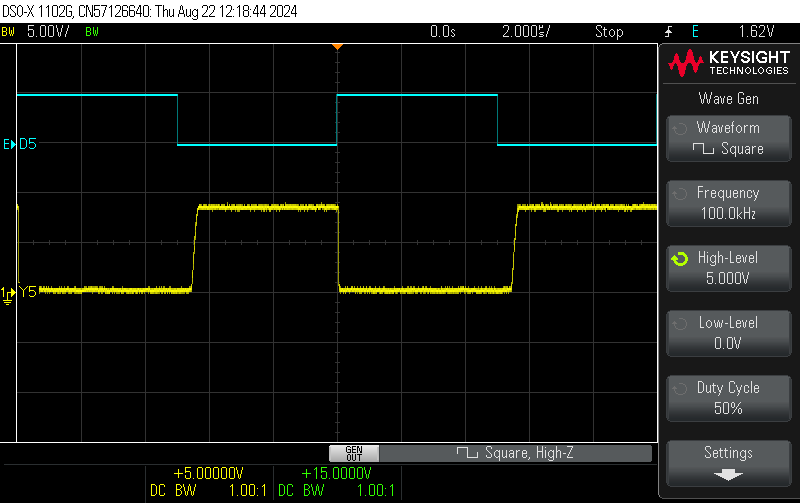 |
| On/Off Delay between BD5026 input D5
and the Flip Flop based output Y6. DUT: BD5026 7542 @ VCC = 9 V, TPULSE = 0.5 ms, RLOAD = 220 Ohm / ILOAD = 40 mA. 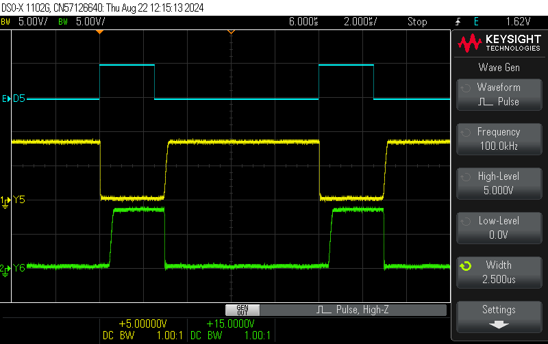 |
| Close-up
of the On Delay between BD5026 input D5 and its direct output Y5. DUT: BD5026 7542 @ VCC = 9 V, TPULSE = 0.5 ms, RLOAD = 220 Ohm / ILOAD = 40 mA. 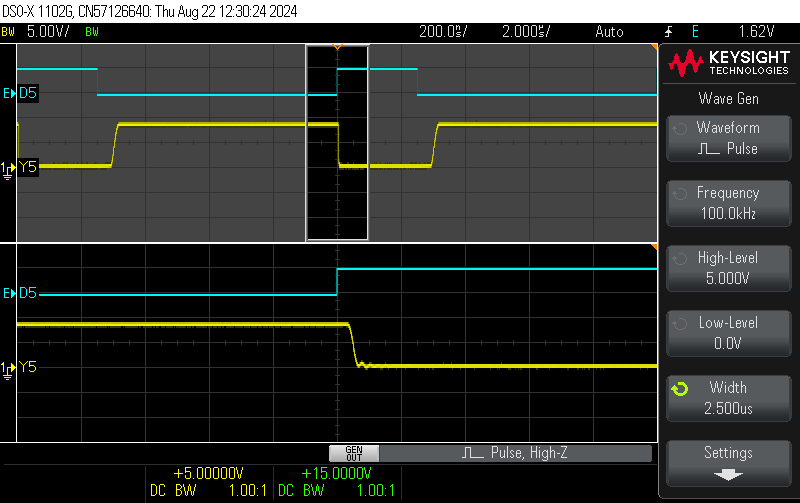 |
| Close-up
of the Off Delay between BD5026 input D5 and its direct output Y5. DUT: BD5026 7542 @ VCC = 9 V, TPULSE = 0.5 ms, RLOAD = 220 Ohm / ILOAD = 40 mA. 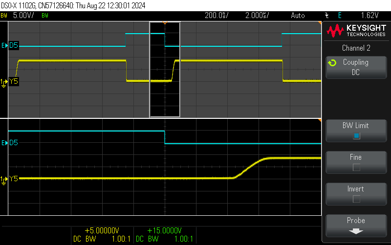 |
| Close-up
of the On Delay between BD5026 input D5 and the Flip Flop based output Y6. DUT: BD5026 7542 @ VCC = 9 V, TPULSE = 0.5 ms, RLOAD = 220 Ohm / ILOAD = 40 mA. 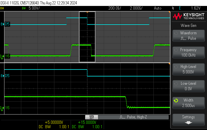 |
| Close-up
of the Off Delay between BD5026 input D5 and the Flip Flop based output
Y6. DUT: BD5026 7542 @ VCC = 9 V, TPULSE = 0.5 ms, RLOAD = 220 Ohm / ILOAD = 40 mA. 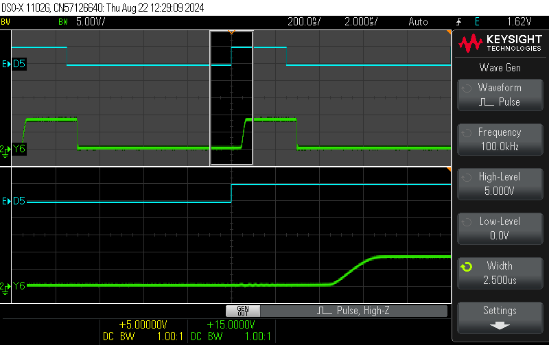 |
If you have additions to the above article please email: joerg@datamath.org.
©