DATAMATH CALCULATOR MUSEUM
|
DATAMATH CALCULATOR MUSEUM |
The SN75494 provides the same basic function as the SN75492 but with some key differences:
|
• Operates from lower VCC voltages, as low as 3.2 V • The SN75494 provides access to the pre-driver collectors via the VCC pin to allow good saturation of the output transistors • An enable input is provided to allow display blanking |
The
SN75494 is preferred on designs running on 3 batteries and is typically found in early designs with additional segment drivers (TMS0120).
QUICK-LINK to Display Drivers.
SR-10 and other early LED calculators
| Item | Min | Typ | Max | Unit | Comments |
| VCC | 3.2 | 7.2 | 8.8 | V | |
| VSS | 6.5 | 7.2 | 8.8 | V | |
| IL | 250 | mA | VI=6.5 V, VO=3.5 V | ||
| IL | 0.2 | mA | Output Leakage Current | ||
| VI-VD | 10 | V |
The SN75494 was manufactured in a 10 um metal gate Bipolar process (metal width = 0.4 mil / 10 um, metal spacing = 0.4 mil / 10 um).
The die size of the SN75494 is approximately tbd mils * tbd mils / tbd mm * tbd mm.
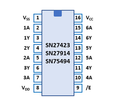
The SN75494 uses a standard 0.3” wide 16-pin DIP (Dual In-line Package with a 0.1” / 2.54 mm lead pitch).
| Pin | IO | Function | Pin | IO | Function |
| 1 | V | VSS | 16 | V | VCC |
| 2 | I | Digit input 1 | 15 | I | Digit input 6 |
| 3 | O | Digit output 1 | 14 | O | Digit output 6 |
| 4 | O | Digit output 2 | 13 | O | Digit output 5 |
| 5 | I | Digit input 2 | 12 | I | Digit input 5 |
| 6 | O | Digit output 3 | 11 | O | Digit output 4 |
| 7 | I | Digit input 3 | 10 | I | Digit input 4 |
| 8 | V | VDD | 9 | I | Enable drivers |
If you have additions to the above datasheet please email: joerg@datamath.org.
© Joerg Woerner, February 02, 2001. No reprints
without written permission.