DATAMATH CALCULATOR MUSEUM
|
|
DATAMATH CALCULATOR MUSEUM |
Additional Pictures
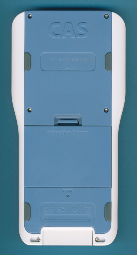
| The backside
of the TI-Nspire CAS+ prototype looks identical to the released TI-Nspire CAS.
|
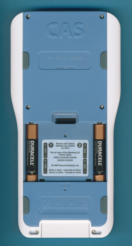
The 4 AAA-sized
batteries of the TI-Nspire CAS+ prototype are accessible from the backside of the calculator.
|
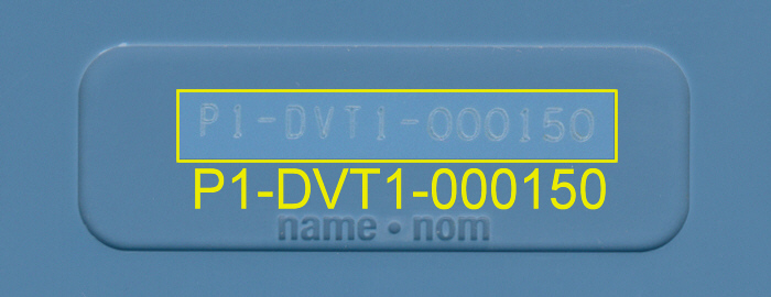
| We
learned how to read the label of this TI-Nspire
CAS+ protoype: Design Validation Test, First Series, Serial #150.
|
|
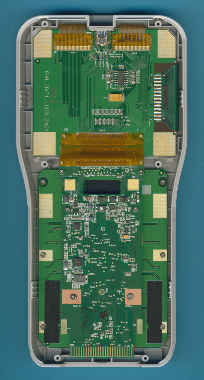
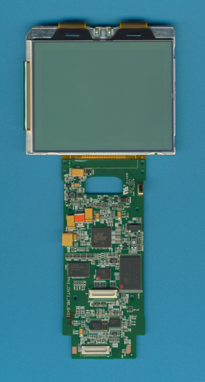
| The internal
construction of the TI-Nspire CAS+ makes use of just 3 printed circuit boards
(PCB's), one for the gray-scale LC-Display and power supply, one for the computing unit and the keyboard.
|
|
| The frontside of the
PCB's reveal the construction of the 240 * 320 pixel gray-scale LC-Display, the TI-OMAP and a total of three different memory chips.
|
|
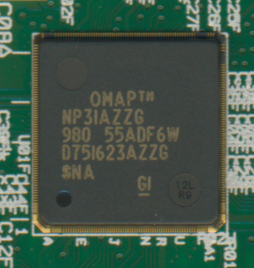
| The brain of the
TI-Nspire CAS+ prototype is actually a System-on-Chip based on the OMAP architecture from Texas Instruments. We assume that the tiny housing hosts a 78 MHz ARM9 32-bit RISC processor.
|
|
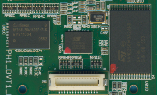
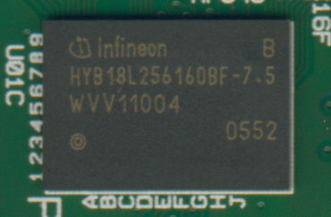
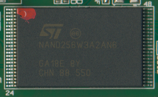
| The TI-Nspire
CAS+ uses three
different memory chips, a 256k*16 NOR Flash-ROM, 32M Bytes
NAND Flash-ROM, and 16M*16 SDRAM. The clock frequency of the SoC is 12 MHz.
|
|
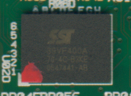
| Additional Zoom-Images -
NOR Flash-ROM:
|
Additional Zoom-Images -
SDRAM:
|
| Additional
Zoom-Images - NAND Flash-ROM:
|
|
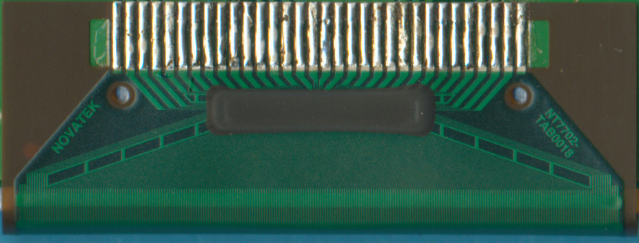
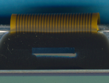
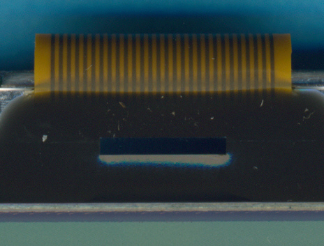
| The 320 *
240 pixel gray-scale LC-Display needs a total of three drivers. We located this Novatek NT7702 row-driver and two unidentified column-drivers.
|
|
If you have additions to the above article please email: joerg@datamath.org.
© Joerg Woerner, August 2, 2009. No reprints without written permission.