DATAMATH CALCULATOR MUSEUM
|
|
DATAMATH CALCULATOR MUSEUM |
Datamath Calculator Museum DCM-50A Playground Clock Recovery Module
| Date of introduction: | January 25, 2025 | Display technology: | n.a. |
| New price: | Display size: | n.a. | |
| Size: | 2.4" x 2.6" x 1.00" 61 x 66 x 25 mm3 |
||
| Weight: | 1.0 ounces, 28 grams | Serial No: | 0001 |
| Batteries: | n.a. | Date of manufacture: | mth 01 year 2025 |
| AC-Adapter: | n.a. | Origin of manufacture: | USA |
| Precision: | Integrated circuits: | CD4066, CD40106, 2*CD4522 | |
| Memories: | |||
| Program steps: | Courtesy of: | Joerg Woerner |
![]()
 When
Texas Instruments introduced with the TMS0100
their first generation single-chip calculator circuit, it didn't include the
oscillator for its internal electronics and the Datamath Calculator Museum
DCM-50A
Platform features consequently an astable mutlivibrator with 250 kHz to
operate the chip. Later designs like the
TMS0800 or TMS1000 incoporated an
internal oscillator that could be enabled but needed either an external resistor
or an arrangement of an external resistor and capacitor, both types are
supported by the DCM-50A Platform.
When
Texas Instruments introduced with the TMS0100
their first generation single-chip calculator circuit, it didn't include the
oscillator for its internal electronics and the Datamath Calculator Museum
DCM-50A
Platform features consequently an astable mutlivibrator with 250 kHz to
operate the chip. Later designs like the
TMS0800 or TMS1000 incoporated an
internal oscillator that could be enabled but needed either an external resistor
or an arrangement of an external resistor and capacitor, both types are
supported by the DCM-50A Platform.
On our mission to Characterize and Reverse-Engineer not only calculator chips manufactured by Texas Instruments, but branching out to offerings from their competitors in the 1970s, namely AMI, Cal-Tex, Commodore/MOS Technology, Electronic Arrays, General Instrument, Hitachi, Litronix, Matsushita, Mitsubishi, Mostek, National Semiconductor, NEC, Omron, RFT, Rockwell, Sharp, Toshiba, and Western Digital, we developed the DCM-50A (PLAYGROUND) with its modular approach. As expected did we encounter in the meantime even more clock oscillator designs and we differentiate between four architectures:
| • 1 - External clock oscillator • 2 - Internal Clock oscillator with optional external clock input • 3 - Internal Clock oscillator w/o optional external clock input but clock output • 4 - Internal Clock oscillator w/o optional external clock input and w/o clock output |
In the process of the Characterization of single-chip calculator circuits is it beneficial to have access to the internal clock of the Device-under-Test. Most output signals are generated based on either the rising or falling edge of these internal clock signals and some signals like keyboard scanning or display scanning are often derived from the internal clock frequency.
Here at the Datamath Calculator Museum we are using the Digilent Digital Discovery™, a combined logic analyzer, protocol analyzer, and pattern generator instrument, to generate the clock signals for the Device-under-Test - an approach that works perfectly for the first three of the above mentioned clock oscillator architectures.
Studying some single-chip calculator circuits of Architecture #4, devices that use an internal clock oscillator that can't be accessed or overridden, we started to extract their internal clock frequency with measuring the small modulation of their supply currents and compared it with their display scan frequency. All analyzed devices had a constant relationship between display scan frequency and clock frequency, actually an integer value between 8 and 26 clock cycles per digit position.
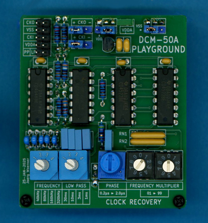
 Based on this observation we developed the DCM-50A Playground Clock Recovery Module,
a small printed circuit board (PCB) to re-create the internal clock oscillator
frequency of single-chip calculator circuits from their display scanning timing.
Basic idea of this approach is multiplying the frequency of "Digit Pulses" from
the Device-under-Test by an Integer value between 2 and 99 with the means of a
Voltage Controlled Oscillator (VCO), a Phase-Locked-Loop (PLL) and a
Programmable Divider. The "Digit Pulses" are generated on
the
DCM-50A Playground DIL42 Adapter from the Digit Outputs with
a Diode "Wired Or"
arrangement and fed through the Clock-Input (CKI) Header with selectable
polarity to the phase comparator of the PLL. The center frequency of the VCO can
be selected in four steps between 40 kHz and 320 kHz and has a frequency range of
+/- 50%, covering a total range between 20 kHz and 480 kHz. The output frequency
of the VCO is made available on the Clock-Output (CKO) Header with selectable
polarity and an adjustable Phase Delay between 0.2 us and 2.0 us. Additionally
is the VCO output frequency brought to a programmable 2-digit divider with its
output fed into the second input of the phase comparator of the PLL. The output
of the phase comparator controls - filtered with an adjustable low-pass with a
time constant between 1 ms and 30 ms - the VCO frequency accordingly. The DCM-50A Playground Clock
Recovery Module plugs with three Jumper-Headers over the TMS1000 ZIF-Socket and
generates its own supply voltage of 9 Volts from the VSS and VGG voltages of the DCM-50A Platform.
Based on this observation we developed the DCM-50A Playground Clock Recovery Module,
a small printed circuit board (PCB) to re-create the internal clock oscillator
frequency of single-chip calculator circuits from their display scanning timing.
Basic idea of this approach is multiplying the frequency of "Digit Pulses" from
the Device-under-Test by an Integer value between 2 and 99 with the means of a
Voltage Controlled Oscillator (VCO), a Phase-Locked-Loop (PLL) and a
Programmable Divider. The "Digit Pulses" are generated on
the
DCM-50A Playground DIL42 Adapter from the Digit Outputs with
a Diode "Wired Or"
arrangement and fed through the Clock-Input (CKI) Header with selectable
polarity to the phase comparator of the PLL. The center frequency of the VCO can
be selected in four steps between 40 kHz and 320 kHz and has a frequency range of
+/- 50%, covering a total range between 20 kHz and 480 kHz. The output frequency
of the VCO is made available on the Clock-Output (CKO) Header with selectable
polarity and an adjustable Phase Delay between 0.2 us and 2.0 us. Additionally
is the VCO output frequency brought to a programmable 2-digit divider with its
output fed into the second input of the phase comparator of the PLL. The output
of the phase comparator controls - filtered with an adjustable low-pass with a
time constant between 1 ms and 30 ms - the VCO frequency accordingly. The DCM-50A Playground Clock
Recovery Module plugs with three Jumper-Headers over the TMS1000 ZIF-Socket and
generates its own supply voltage of 9 Volts from the VSS and VGG voltages of the DCM-50A Platform.
The schematics and layout of the DCM-50A Playground Clock Recovery Module are providing accordingly:
| • VSS and VGG access from
Jumper-Header J23 and J26, respectively • Pin-Header to recreate J23 and J26 • Voltage regulator to generate the Analog VDDA voltage (-9 V) • LED to signal the VDDA voltage • Pin-Header to access CKO, VSS, CKI, VDDA and Test Points PP and LP • Pin-Header to select CKI and CKO Polarity • 4-position Rotary Switch (blue) to select the VCO Center Frequency 40 kHz/ 80 kHz / 160 kHz / 320 kHz • 4-position Rotary Switch (blue) to select the Low-Pass Filter Time Constant 30 ms / 10 ms / 3 ms / 1ms • Potentiometer to adjust the Phase Delay 0.2 us - 2.0 us • 2*10-position Rotary Switch (black) to program the Frequency Multiplier '02' - '99' |
Please notice that the DCM-50A Playground Clock Recovery Module needs to be plugged over the TMS1000 ZIF-Socket into the three Jumper-Headers J21, J23 and J26 on the DCM-50A Platform.
If you have additions to the above article please email: joerg@datamath.org.
© Joerg Woerner, January 28, 2025. No reprints without written permission.