DATAMATH CALCULATOR MUSEUM
|
DATAMATH CALCULATOR MUSEUM |
Fairchild Semiconductor developed early in the 1970s a family of micro-programmed MOS/LSI (Metal–oxide Semiconductor/Large Scale Integration) processor blocks called PPS 25 (Programmed Processor System - 25 Digits) to bridge the gap between simple electronic calculators and microcomputers. A minimal PPS 25 design uses six Micromosaic chips interconnected by 4-bit data buses and various control signals, corresponding directly to the block diagram of a computer based on the Harvard architecture.
At the core of the system is the CPU, composed of the 3805 Arithmetic/Logic Unit and the 3806 Control Unit. The 3808 and 3809 Data Memories each provide three dynamic 25-digit shift registers, while the 3810 Program Memory provides 256 Words * 12 Bits of storage. The 3803 and 3807 Input Device chips support up to 32 keys and 16 switches each, and the 3811 Output Device drives displays of up to 16 Digits.
The 3806 Function and Timing Unit provides the address and control logic for the PPS 25 System and is providing its traffic control, in that it contains the master timing counter and generates the Sync signal. For example, the time enable portion of the instruction is used to select the portion of the word upon which a given command is to be executed. There are six programmable time enable patterns available, each called up by a different code. Additional status registers are used for storing return addresses for subroutine calls, storing program flags, and storing mode control switch status.
The 3807 Function and Timing Unit is combining the following features in one 24-pin package:
|
• Instruction Address
Register • Micro-instruction Address Adder • Program Branch Decision Logic • Two 25-bit Status Registers • Pointer and Status Counters • 25 * 6 Bits Time Enable Pattern ROM • Master Timing Circuit • 4-level Nested Subroutine Linkage • Interface to 3805 Arithmetic Chip |
QUICK-LINK to PPS 25 Building Blocks.
| Type | Year | Function | Products | Comments |
| 3806 (SL30342) | 1973 | Function and Timing Unit |
Centurion Industries Multiputer
CPD-15, CPD-35 Cybernetic Systems Mathiputer CPD-15, CPD-35 |
24 pin Ceramic DIP |
| Description | Comments | |
| Architecture | Harvard, Processor Blocks | First Generation |
| Category | Register Processor | 25-digit BCD-serial |
| ROM Size | not applicable | |
| RAM Size | 150 Bits | 1 Register * 100 Bits (25 Digits) 2 Registers * 25 Bits |
| Item | Min | Typ | Max | Unit | Comments |
| VSS | 4.75 | 5.0 | 5.25 | V | TTL, DTL compatible |
| VDD | 0 | V | |||
| VGG | -9.5 | -10.0 | -10.5 | V | |
| VOH1 | 2.4 | VSS | V | 1 TTL Load | |
| VOL1 | 0 | 0.4 | V | 1 TTL Load | |
| VOH2 | VSS-1.0 | VSS | V | MOS Load | |
| VOL2 | 0 | 0.5 | V | MOS Load | |
| VIH1 | VSS-1.0 | VSS | V | DTL/TTL compatible | |
| VIL1 | VDD | VSS-4.2 | V | DTL/TTL compatible | |
| VIH2 | VSS-1.0 | VSS | V | Clock Input | |
| VIL2 | VGG | VSS-14.0 | V | Clock Input | |
| Ext. CK | 400 | kHz | Two-phase clock | ||
| CP1 Width | us | Active low | |||
| CP2 Width | us | Active low | |||
| CP1 to CP2 Delay | us | Between pulses |
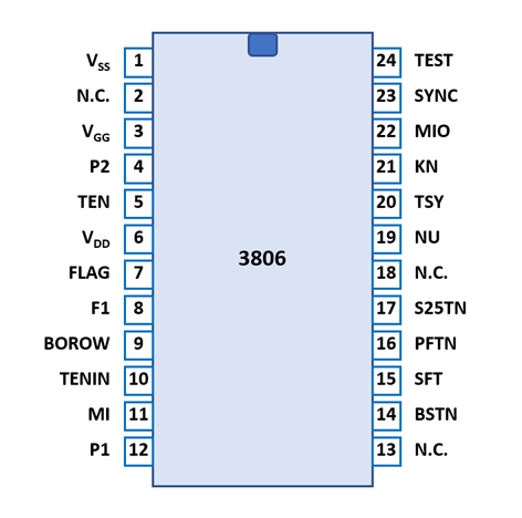
The 3806 (SL30342) Function and Timing Unit uses a standard 0.6” wide 24-pin CDIP (Ceramic Dual In-line Package with a 0.1” / 2.54 mm lead pitch).
The die of the 3806 (SL30342) Function and Timing Unit is attached to the gold-plated cavity of the 24-pin CDIP with its Pin 1 (VSS) bonded to the substrate and silicon die. Pins 2, 3, and 18 are not bonded to the silicon die.
The PPS 25 Building Blocks were manufactured in a 11.5 um metal gate PMOS process (metal width = 0.45 mil / 11.5 um, metal spacing = 0.44 mil / 11.5 um, diffusion width = 0.30 mil / 8.0 um, diffusion spacing = 0.30 mil / 8.0 um). The die size of the 3806 (SL30342) Function and Timing Unit is approximately 170 mils * 170 mils / 4.3 mm * 4.3 mm.
| PPS 25 - 3806 (SL30342) Function and Timing Unit | |||||
| Pin | IO | Function | Pin | IO | Function |
| 1 | V | Positive Voltage VSS | 24 | I | TEST |
| 2 | N.C. | 23 | O | SYNC | |
| 3 | V | Negative Voltage VGG | 22 | O | Micro Instruction Output MIO |
| 4 | O | Clock P2 | 21 | I | Direct Input Line KN |
| 5 | O | Time Enable ROM | 20 | I | TSY |
| 6 | V | Common Voltage VDD | 19 | I | NU |
| 7 | I | Adder FLAG | 18 | N.C. | |
| 8 | I | External Device Ready | 17 | O | S25TN |
| 9 | I | Adder BOROW | 16 | O | PFTN |
| 10 | I | Time Enable In ROM | 15 | O | SFT |
| 11 | I | Micro Instruction Input MI |
14 | O | BSTN |
| 12 | I | Clock P1 | 13 | N.C. | |
If you have additions to the above datasheet please email: joerg@datamath.org.
© Joerg Woerner, May 8, 2026. No reprints
without written permission.