DATAMATH CALCULATOR MUSEUM
|
DATAMATH CALCULATOR MUSEUM |
Fairchild Semiconductor developed early in the 1970s a family of micro-programmed MOS/LSI (Metal–oxide Semiconductor/Large Scale Integration) processor blocks called PPS 25 (Programmed Processor System - 25 Digits) to bridge the gap between simple electronic calculators and microcomputers. The PPS 25 adopts a Harvard architecture and utilizes dynamic 25-digit shift registers for its data storage, enabling both precise and fast mathematical operations. The PPS 25 Building Blocks are based on Fairchild's Micromosaic "standard cell" technology, originally developed for GE's Avionics and formally introduced in 1969. This design methodology for application-specific integrated circuits (ASICs) is based on pre-designed, pre-characterized dynamic logic blocks (such as AND, OR, shift registers, RAM, ROM). These cells, arranged in rows with fixed height and variable width, could be automatically interconnected, enabling a balance between high performance and efficient fabrication.
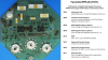
A minimal PPS 25 design uses six Micromosaic chips interconnected by 4-bit data buses and various control signals, corresponding directly to the block diagram of a computer based on the Harvard architecture.
At the core of the system is the CPU, composed of the 3805 Arithmetic/Logic Unit and the 3806 Control Unit. The 3808 and 3809 Data Memories each provide three dynamic 25-digit shift registers, while the 3810 Program Memory provides 256 Words * 12 Bits of storage. The 3803 and 3807 Input Device chips support up to 32 keys and 16 switches each, and the 3811 Output Device drives displays of up to 16 Digits.
The clock frequency of PPS 25 Building Blocks is 400 kHz, resulting in a Digit Time of 2.5 us and a Word Time of 62.5 us. The up to seven 25-digit Registers of a PPS 25 system can be used for one 16-digit number or two 10-digit numbers, allowing for high-end desktop or scientific calculators. Up to 26 ROM (Read-Only Memory) chips can be addressed by the PPS 25 CPU for a combined 3,328 Words * 12 Bits capacity and the two Input chips allow the support of keyboards with up to 61 keys and 32 mode switches. Eight PPS 25 Building Blocks were offered, both the 3806 Function and Timing Unit and 3810 ROM could be customized:
|
• 3803 Input Device – Expander for 3807 Keyboard Scanner • 3805 Arithmetic Chip – Adder/Subtractor and 25-digit BCD Register A • 3806 Function and Timing Unit - Program Counter, Branch Logic, two 25-bit Status Registers and generates the Master timing • 3807 Input Device – 4 Keyboard Scan Outputs, 16 Inputs for 32 keys with two-key rollover with 5-bit Key-code and 16 switches • 3808 Memory Register – Three 25-digit BCD Register B, C, and D • 3809 Memory Register – Three 25-digit BCD Register E, F, and G • 3810 ROM – 256 * 12 Bits Micro Instruction Memory, up to 26 ROM Chips • 3811 Output Device – 16-digit BCD Data Register, multiplexing, leading zero suppression and blanking of the display |
The PPS 25 was introduced in 1971/1972 and de-emphasized around 1974 in favor of the F8 processor.
 As of today, we are aware of only one PPS 25-based design that comes close to an electronic calculator; however, it is at least used in classrooms.
QUICK-LINK to Fairchild Calculator Integrated Circuits.
MANUFACTURER DOCUMENTATION (Courtesy of Bitsavers):
|
•
Fairchild Semiconductor OPTIMOS (September 1972) • PPS 25 Preliminary Users Manual (October 1972) |
| Type | Year | Function | Products | Comments |
| 3805 | 1973 | Arithmetic Chip |
Centurion Industries Multiputer
CPD-15, CPD-35 Cybernetic Systems Mathiputer CPD-15, CPD-35 |
18-pin Ceramic DIP |
| 3806 (SL30342) | Function and Timing Unit | 24-pin Ceramic DIP | ||
| 3807 | Input Device | 40-pin Ceramic or Plastic DIP | ||
| 3809 | Memory Register | 16-pin Ceramic DIP | ||
| 3810 (SL30745) | ROM | 16-pin Ceramic DIP | ||
| 3811 | Output Device | 24-pin Ceramic DIP |
| Description | Comments | |
| Architecture | Harvard, Processor Blocks | First Generation |
| Category | Register Processor | 25-digit BCD-serial |
| Related | ||
| ROM Size | 3,072 - 79,872 Bits | 256 - 6,656 Words * 12 Bits |
| RAM Size | 150 -750 Bits | 1 - 7 Registers * 100 Bits (25 Digits) 2 Registers * 25 Bits |
| Outputs | 4 Digit Select 4 BCD Data 3 Discrete Outputs 4 - 8 Keyboard Scan |
External Digit Decoder External Segment Decoder Memory, Sign, Decimal |
| Inputs | 8 - 16 Key
Inputs 8 - 16 Switch Inputs |
Up to 61 keys Up to 32 switches |
| Item | Min | Typ | Max | Unit | Comments |
| VSS | 4.75 | 5.0 | 5.25 | V | TTL, DTL compatible |
| VDD | 0 | V | |||
| VGG | -9.5 | -10.0 | -10.5 | V | |
| VOH1 | 2.4 | VSS | V | 1 TTL Load | |
| VOL1 | 0 | 0.4 | V | 1 TTL Load | |
| VOH2 | VSS-1.0 | VSS | V | MOS Load | |
| VOL2 | 0 | 0.5 | V | MOS Load | |
| VIH1 | VSS-1.0 | VSS | V | DTL/TTL compatible | |
| VIL1 | VDD | VSS-4.2 | V | DTL/TTL compatible | |
| VIH2 | VSS-1.0 | VSS | V | Clock Input | |
| VIL2 | VGG | VSS-14.0 | V | Clock Input | |
| Ext. CK | 400 | kHz | Two-phase clock | ||
| CP1 Width | us | Active low | |||
| CP2 Width | us | Active low | |||
| CP1 to CP2 Delay | us | Between pulses |
If you have additions to the above datasheet please email: joerg@datamath.org.
© Joerg Woerner, May 8, 2026. No reprints
without written permission.