DATAMATH CALCULATOR MUSEUM
|
DATAMATH CALCULATOR MUSEUM |
Fairchild Semiconductor developed early in the 1970s a family of micro-programmed MOS/LSI (Metal–oxide Semiconductor/Large Scale Integration) processor blocks called PPS 25 (Programmed Processor System - 25 Digits) to bridge the gap between simple electronic calculators and microcomputers. A minimal PPS 25 design uses six Micromosaic chips interconnected by 4-bit data buses and various control signals, corresponding directly to the block diagram of a computer based on the Harvard architecture.
At the core of the system is the CPU, composed of the 3805 Arithmetic/Logic Unit and the 3806 Control Unit. The 3808 and 3809 Data Memories each provide three dynamic 25-digit shift registers, while the 3810 Program Memory provides 256 Words * 12 Bits of storage. The 3803 and 3807 Input Device chips support up to 32 keys and 16 switches each, and the 3811 Output Device drives displays of up to 16 Digits.
The basic keyboard device is the 3807, it is generating a 5-bit code for each key that makes a transition from an inactive state to an active state. This 5-bit code is stored on the 3807 Input Device until a command occurs in the program, instructing it to transmit the 5-bit code to the 3806 Function and Timing Unit. In addition the 3807 Input Device is scanning up to 16 static switches. The 3803 Input Device extends the keyboard capabilities beyond 32 keys.
The 3807/3803 Input Device chips are combining the following features in one 40-pin package:
|
• Four Scanning Outputs D1-D4
for up to 32 keys and 16 switches • Eight Key Matrix Inputs R1-R8 • Eight Switch Matrix Inputs S1-S8 • Alarm Input Lock • Direct Key Output KN • Serial Micro Instruction Input MI • Anti-bounce Feature • Two-key rollover (legato) |
QUICK-LINK to PPS 25 Building Blocks.
| Type | Year | Function | Products | Comments |
| 3807 | 1973 | Input Device |
Centurion Industries Multiputer
CPD-15, CPD-35 Cybernetic Systems Mathiputer CPD-15, CPD-35 |
40 pin Ceramic or Plastic DIP |
| Item | Min | Typ | Max | Unit | Comments |
| VSS | 4.75 | 5.0 | 5.25 | V | TTL, DTL compatible |
| VDD | 0 | V | |||
| VGG | -9.5 | -10.0 | -10.5 | V | |
| VOH1 | 2.4 | VSS | V | 1 TTL Load | |
| VOL1 | 0 | 0.4 | V | 1 TTL Load | |
| VOH2 | VSS-1.0 | VSS | V | MOS Load | |
| VOL2 | 0 | 0.5 | V | MOS Load | |
| VIH1 | VSS-1.0 | VSS | V | DTL/TTL compatible | |
| VIL1 | VDD | VSS-4.2 | V | DTL/TTL compatible | |
| VIH2 | VSS-1.0 | VSS | V | Clock Input | |
| VIL2 | VGG | VSS-14.0 | V | Clock Input | |
| Ext. CK | 400 | kHz | Two-phase clock | ||
| CP1 Width | us | Active low | |||
| CP2 Width | us | Active low | |||
| CP1 to CP2 Delay | us | Between pulses |
The 3807 Keyboard Device uses a standard 0.6” wide 40-pin CDIP (Ceramic Dual In-line Package with a 0.1” / 2.54 mm lead pitch).
The die of the 3807 Keyboard Device is attached to the gold-plated cavity of the 40-pin CDIP with its Pin 3 (VSS) bonded to the substrate and silicon die. Pins 6, 15, 17, 19, 20, 21, 24, 25, 26, and 36 are not bonded to the silicon die.
The PPS 25 Building Blocks were manufactured in a 11.5 um metal gate PMOS process (metal width = 0.45 mil / 11.5 um, metal spacing = 0.45 mil / 11.5 um, diffusion width = 0.30 mil / 8.0 um, diffusion spacing = 0.30 mil / 8.0 um). The die size of the 3807 Keyboard Device is approximately 145 mils * 150 mils / 3.7 mm * 3.9 mm.
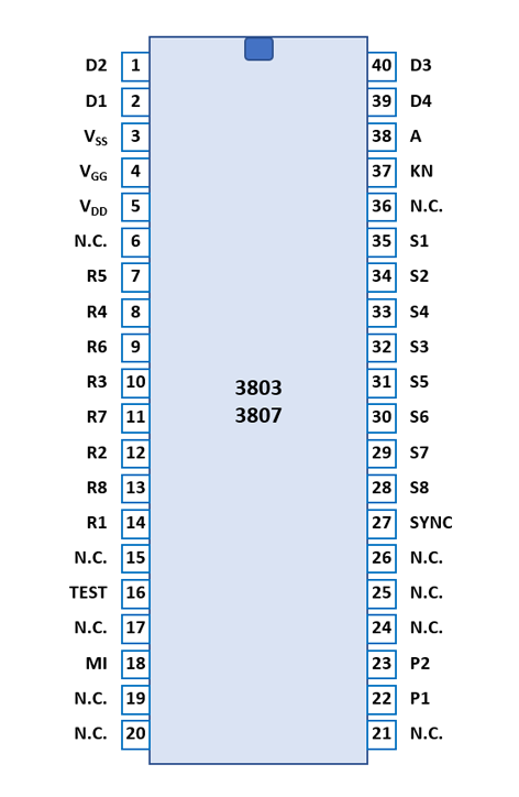
| PPS 25 - 3803/3807 Keyboard Device | |||||
| Pin | IO | Function | Pin | IO | Function |
| 1 | O | Scan Output D2 | 40 | O | Scan Output D3 |
| 2 | O | Scan Output D1 | 39 | O | Scan Output D4 |
| 3 | V | Positive Voltage VSS | 38 | O | Alarm Input Lock |
| 4 | V | Negative Voltage VGG | 37 | O | Key Output KN |
| 5 | V | Common Voltage VDD | 36 | N.C. | |
| 6 | N.C. | 35 | I | Switch Input S1 | |
| 7 | I | Key Input R5 | 34 | I | Switch Input S2 |
| 8 | I | Key Input R4 | 33 | I | Switch Input S4 |
| 9 | I | Key Input R6 | 32 | I | Switch Input S3 |
| 10 | I | Key Input R3 | 31 | I | Switch Input S5 |
| 11 | I | Key Input R7 | 30 | I | Switch Input S6 |
| 12 | I | Key Input R2 | 29 | I | Switch Input S7 |
| 13 | I | Key Input R8 | 28 | I | Switch Input S8 |
| 14 | I | Key Input R1 | 27 | I | SYNC |
| 15 | N.C. | 26 | N.C. | ||
| 16 | I | TEST | 25 | N.C. | |
| 17 | N.C. | 24 | N.C. | ||
| 18 | I | Micro Instruction Input MI |
23 | I | Clock P2 |
| 19 | N.C. | 22 | I | Clock P1 | |
| 20 | N.C. | 21 | N.C. | ||
If you have additions to the above datasheet please email: joerg@datamath.org.
© Joerg Woerner, May 8, 2026. No reprints
without written permission.