DATAMATH CALCULATOR MUSEUM
|
DATAMATH CALCULATOR MUSEUM |
The µPD278 single-chip calculator is a member of the µPD946 Series, and offers through its firmware programming a different Feature Set, better aligned to the µPD276 and µPD277 offerings.
|
• µPD277: [+/−] [M=] [MR/C] [- K] [%] [√x] • µPD276: [+/−] [M+=] [M−=] [MRC] [MC] [MR] [- ∑] [- K] [%] [√x] • µPD278: [+/−] [M+=] [M−=] [MRC] [%] [√x] [PI] [X<>Y] • µPD946: [+/−] [M+=] [M−=] [MR] [MC] [ - ∑] [%] [1/x] [x2] [√x] [PI] |
QUICK-LINK to NEC Calculator Integrated Circuits.
| Type | Calculators | Keyboard | Constant (M-D-A-S) |
Digits | Fixed DP | Rounding | Special Functions |
Seg./Dig. Blanking |
(6,7,9) Font |
Entry Overflow |
Calculating Overflow |
| µPD278 | Olympia CD44S | [+][−][=] | 1-2-X-X | 8 | Float | None | [+/−][M+=][M−=] [MR][MC][MRC] [%][√x][PI][X<>Y] |
NONE S1, S16 |
|
||
| Reference µPD946 |
Royal RSC-40 | [+][−][=] | 1-2-2-2 | 8 | Float | None | [+/−][M+=][M−=] [MR][MC][MRC][ - ∑] [%][1/x][x2][√x] [PI] |
NONE S1, S16 |
| Description | Comments | |
| Architecture | Single-chip Calculator | Second Generation |
| Category | Register Processor | Bit-serial |
| Related | µPD946 | Different ROM Programming |
| ROM Size | 8,704 Bits | 512 Words * 17 Bits |
| RAM Size | 260 Bits | 5 Registers * 52 Bits (13 Digits) |
| Outputs | 9 Digits 9 Segments |
VFD Digit Drivers VFD Segment Drivers |
| Inputs | 4 Keyboard 1 Clear |
Segment to Keyboard Scan-Matrix Active High |
Capacity: Up to 8 digits (positive and negative)
Logic: Algebraic Chain Logic with Automatic Constant
[2] [x] [3] [+=] [4] [x] [5] [=] → '50.'
Number Entry: Right-justified number entry, entering a ninth digit is ignored
[1] [2] [3] [4] [5] [6] [7] [8] [9] → '12345678.
Decimal Point: First entered decimal point is used, additional decimal point entries are ignored
[1] [.] [2] [.] [3] → '1.23'
Fixed Decimal Point: Fixed decimal point arithmetic is not supported
Decimal Alignment: Decimal alignment is not supported
[0] [.] [4] [5] [+] [0] [.] [5] [5] [=] → '1.'
Clear: Automatic power-up clear implemented. [C] key clears the whole calculator. First press of the [C/CE] key clears last entry of a number, second press clears the calculator
[1] [+] [2] [C] [3] [=] → '3.'; [1] [+] [2] [C/CE] [3] [=] → '4.'; [1] [+] [2] [C/CE] [C/CE] [3] [=] → '3.'
Change Sign: The change sign function can be used in mid number entry but is cancelled if pressing the [+/−] key before entering the number
[C] [+/−] → '-0.', [2] [x] [3] [=] → '6.'; [2] [+/−] [x] [3] [=] → '-6.'
Number Display: Right-justified number display with leading-zero suppression
Negative Numbers: Negative numbers are shown with '-' in the leftmost position
Calculating Overflow: An overflow shows the result with the decimal point shifted 8 positions to the left and 'C' (or 'E' for negative numbers) in the leftmost position and is recoverable using the [C] or [C/CE] keys
[1] [2] [3] [4] [5] [x] [1] [2] [3] [4] [5] [=] → ''C1.5239902'
Memory: 3-key memory with [M+=], [M−=] and [MRC] keys implemented. Memory store is indicated with '.' in the leftmost position
[MRC] [MRC] [3] [x] [2] [M+=] → '. 6.', [C] → '. 0.', [MRC] → '. 6.', [MRC] → '6.'
Memory Overflow: A memory overflow keeps the stored value in place and is indicated with and 'C.' in the leftmost position. It is only recoverable using the [C] or[C/CE] keys
[MRC] [MRC] [99999998] [+/−] [M+=] → '-.99999998.', [3] [+/−] [M+=] → 'C. 0.', [C] → '. 0.', [MRC] → '-.99999998.'
Divide By Zero: A division of a positive or negative number by zero shows a '0' and 'C' in the leftmost position and is only recoverable using the [C] or [C/CE] keys
[1] [:] [0] [=] → 'C 0.'; [−] [1] [:] [0] [=] → 'C 0.'
Timeout: Not supported
Rounding: Rounding of displayed calculating results is not supported
[2] [0] [:] [3] [=] → '6.6666666'
Automatic Constant: Implemented for multiplication (1st number used as constant) and division (2nd)
[3] [x] [2] [=] [=] → '18.', [1] [=] → '3.'; [4] [x] [=] [=] → '64.'
[3] [:] [2] [=] [=] → '0.75', [1] [=] → '0.5.'; [4] [:] [=] [=] → '0.0625'
[3] [+] [2] [=] [=] → '7.', [1] [=] → '3.'; [4] [+] [=] [=] → '12.'
[3] [−] [2] [=] [=] → '-1.', [1] [=] → '-1.'; [4] [−] [=] [=] → '-4.'
Percent Function: The [%] key following the [x] key allows with the [+] and [−] keys mark-up and discount calculations
[2] [0] [x] [5] [%] → '1.', [=] → '20.'
[2] [0] [x] [5] [%] → '1.', [+] [=] → '21.'
[2] [0] [x] [5] [%] → '1.', [−] [=] → '19.'
[5] [:] [2] [0] [%] → '25.', [=] → '1.25'
Negative Square Root: Negative square roots are not allowed and result in an overflow condition indicated with an 'C' in the leftmost position and is only recoverable with the [C] or [C/CE] keys
[8] [√x] → '2.8284271'; [−] [8] [√x] → 'C 0.'
Register Exchange: The [X<>Y] keys allows the exchange of the display register with the operand register
[1] [:] [2] → '2.', [X<>Y] → '1.', [=] → '2.'
Known Calculator Logic Bugs: None
ABSOLUTE MAXIMUM RATINGS
| Item | Min | Typ | Max | Unit | Comments |
| VDD | -15.0 | 0.3 | V | to VSS | |
| VGG | -15.0 | 0.3 | V | to VSS | |
| VOUT | -30.0 | 0.3 | V | VFD Output Voltage through 50 kOhm Resistors | |
| VIN (AC, CH1, CH2, CG) |
-15.0 | 0.3 | V | Input Voltage through 50 kOhm Resistors | |
| VIN (NK, FK1, FK2) |
-30.0 | 0.3 | V | Input Voltage through 50 kOhm Resistors |
RECOMMENDED OPERATING CONDITIONS
| Item | Min | Typ | Max | Unit | Comments |
| VSS | 0 | V | |||
| VDD | -4.95 | -4.5 | -4.05 | V | |
| VGG | -9.9 | -9.0 | -8.1 | V | |
| VOUT | -30.0 | 0 | V | VFD Output Voltage through 100 kOhm Resistors | |
| VIH | -1.8 | 0 | V | Input Voltage through 100 kOhm Resistors | |
| VIL | -30.0 | -6.5 | V | Input Voltage through 100 kOhm Resistors | |
| CCG | 1,500 | pF | CG to VSS |
ELECTRICAL CHARACTERISTICS
| Item | Min | Typ | Max | Unit | Comments |
| IDD | 2.3 | 3.5 | mA | CCG = 1,500 pF, Segment- and | |
| IGG | 1.0 | 1.8 | mA | Digit-Driver Load 100 kOhm to VGG | |
| ION1 | -1.0 | mA | VOT = -1.0 V | ||
| ION2 | -3.0 | mA | VOT = -2.0 V | ||
| IOFF | -10 | uA | VOT = -28.0 V | ||
| IIH | +200 | uA | VIT = -1.8 V | ||
| IIL | -20 | uA | VIT = -24.0 V | ||
| FOSC | 26 | 60 | kHz | CCG = 1,500 pF, |
CLOCK GENERATOR
All devices of the µPD278 of single-chip calculator circuit include an internal clock oscillator that can be enabled by connecting Pin 28 (CLK/CEXT) with a capacitor CEXT to VSS. Connecting Pin 28 directly to an external clock source overrides the internal clock oscillator and the chip can be operated with frequencies between 20 kHz and about 100 kHz. The external clock frequency should have a duty cycle close to 50% and oscillate between VSS and VDD.
The frequency of the internal clock oscillator is set with the external capacitor CEXT with a nominal value of 1,500 pF, respectively for a typical frequency of 60 kHz. Here at the Datamath Calculator Museum we operate the µPD278 Devices-under-Test (DUT) with an external 1,500 pF capacitor but verify its operation between 700 pF and 2,500 pF.
The operating frequency of the internal clock oscillator depends not only on the external capacitor, but its supply voltages VDD and VGG, too. We observed with our DUT a slightly negative gradients of the oscillation frequency VGG variations and negligible changes over or VDD variations.
INTER-DIGIT BLANKING
The µPD278 single-chip calculator circuit is blanking its Digit Outputs for one State Time before (S1) and after (S16) the Segment Output change, while scanning the keyboard and display.
TEST MODE
The chip design of the µPD946 Series of single-chip calculator circuits and its µPD278 derivate includes an (undocumented) Test Mode that can be activated with two external Pins, namely AC (Pin 25) and CH1 (Pin 1). In normal Calculator Mode Pin 25 is tied to VGG and Pin 1 is tied to VSS, the three other combinations are used for the Test Modes:
| AC (Pin 25) |
CH1 (Pin 1) |
µPD278 Mode |
| VGG | VSS | Calculator Mode |
| VSS | VSS | Test Mode 1 |
| VGG | VGG | Test Mode 2 |
| VSS | VGG | Test Mode 3 |
 Test Mode 1:
Observing the clock input, keyboard scanning inputs K0 to K3, digit-driver outputs D1 to D9
and segment-driver outputs SA to SH and SDP in Test Mode 1 shows activities
on all segment-driver outputs while the digit-driver outputs are disabled.
Test Mode 1:
Observing the clock input, keyboard scanning inputs K0 to K3, digit-driver outputs D1 to D9
and segment-driver outputs SA to SH and SDP in Test Mode 1 shows activities
on all segment-driver outputs while the digit-driver outputs are disabled.
 Test Mode 2:
Observing the clock input, keyboard scanning inputs K0 to K3, digit-driver outputs D1 to D9
and segment-driver outputs SA to SH and SDP in Test Mode 2 shows strong
activities on the digit-driver outputs D4, D5, D7 and D8while the segment-driver
outputs are disabled.
Test Mode 2:
Observing the clock input, keyboard scanning inputs K0 to K3, digit-driver outputs D1 to D9
and segment-driver outputs SA to SH and SDP in Test Mode 2 shows strong
activities on the digit-driver outputs D4, D5, D7 and D8while the segment-driver
outputs are disabled.
 Test Mode 3:
Observing the clock input, keyboard scanning inputs K0 to K3, digit-driver
outputs D1 to D9 and segment-driver outputs SA to SH and SDP in Test Mode 3
shows periodic activities on the segment-driver outputs SE and SF with all
other outputs static on logic low or
logic high level.
Test Mode 3:
Observing the clock input, keyboard scanning inputs K0 to K3, digit-driver
outputs D1 to D9 and segment-driver outputs SA to SH and SDP in Test Mode 3
shows periodic activities on the segment-driver outputs SE and SF with all
other outputs static on logic low or
logic high level.
The Datamath Calculator Museum DCM-50A (PLAYGROUND) supports the Characterization of the µPD946 Series of single-chip calculator circuits using the DCM-50A Playground DIL42 Adapter mounted on top of the DCM-50A PG Frame Carrier and the voltages VSS set to 6.0V and VDD/VGG set to -5.0V. Alternatively, the more flexible - but less comfortable - DCM-50A Playground BB400 Adapter can be used. While the keyboard of the DCM-50A Platform natively supports the segment scanning approach utilized with the NEC µPD946 Series, is it limited to the segment outputs A to G and DP as known from Texas Instruments' TMS0950 and TMS0970/TMC0900 Product Families. The DCM50A Playground KBD123 Keyboard with Switch Matrix overcomes these limitations of the DCM-50A keyboard and supports the architecture of the µPD946 Series. It is plugged on top of the DCM-50A Platform and centered around a 12x3 switch matrix keyboard with patch field for selector switches with diode matrix. All pins of the matrix (12 Columns, 3 keyboard rows and 1 switch row) are directly accessible on pin headers and can be connected with the matching pins on the DCM50A Playground DIL42 or DCM50A Playground BB400 Daughter Boards.
The µPD278 was manufactured in a 7.5 um metal gate PMOS process (metal width = 0.30 mil / 7.5 um, metal spacing = 0.30 mil / 7.5 um, diffusion width = 0.25 mil / 6.0 um, diffusion spacing = 0.35 mil / 9.0 um).
The die size of the µPD278 is approximately 175 mils * 150 mils / 4.4 mm * 3.8 mm.
The µPD278 uses a standard 0.6” wide 28-pin DIP (Dual In-line Package with a 0.1” / 2.54 mm lead pitch).
|
• VSS/VDD/VGG - Confirmed Pin Function from Die Photo • (VSS/VDD/VGG) - Pin Function from Calculator Schematics • N.C. - Confirmed Pin Function from Die Photo or Pin Measurement • (N.C.) - Pin Function from Calculator Schematics |
| Pin | IO | Function | Pin | IO | Function |
| 1 | I | Test Mode CH1 | 28 | I | CLK/CEXT |
| 2 | O | Digit driver 1 (LSD) | 27 | V | Negative Voltage VGG |
| 3 | O | Digit driver 2 | 26 | V | Negative Voltage VDD |
| 4 | O | Digit driver 3 | 25 | I | Test Mode AC |
| 5 | O | Digit driver 4 | 24 | O | Segment driver A |
| 6 | O | Digit driver 5 | 23 | O | Segment driver B |
| 7 | O | Digit driver 6 | 22 | O | Segment driver C |
| 8 | O | Digit driver 7 | 21 | O | Segment driver D |
| 9 | O | Digit driver 8 (MSD) | 20 | O | Segment driver E |
| 10 | O | Digit driver 9 (sign) | 19 | O | Segment driver F |
| 11 | I | Key-matrix input NK | 18 | O | Segment driver G |
| 12 | I | Key-matrix input FK1 | 17 | O | Segment driver H |
| 13 | I | Key-matrix input FK2 | 16 | O | Segment driver DP |
| 14 | V | Common Voltage VSS | 15 | I | Test Mode CH2 |
| The Segment drivers A-H and DP (Decimal Point) are connected to the display in the pictured way. | 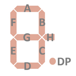 |
The keyboards of all calculators based on the µPD278 single-chip calculator circuits consist of an x/y-matrix connected to nine segment-driver outputs, common voltage VSS and the key-matrix inputs NK, FK1 and FK2.
Display scanning is performed in D1 → D4 → D7 → D2 → D5 → D8 → D3 → D6 → D9 direction at a rate of about 320 Hz. A short pause for parallel keyboard scanning is inserted every three digits:
|
• State Time = 1 Clock =
0.020 ms @ CK=50 kHz • Digit Time = 16 States = 0.320 ms @ CK=50 kHz • Keyboad Time = 4 States = 0.080 ms @ CK=50 kHz • Scan Time = 9 Digit Times + 3 Keyboard Times = 3.120 ms @ CK=50 kHz |
Note: The µPD278 single-chip calculator circuits activate only the necessary digit-driver outputs, while displaying a "0." only D1 would be enabled.
Keyboard scanning of the µPD278 differs from the µPD946: The µPD946 is inserting every three Scan Times a brief sequential keyboard scanning cycle, even if no keypress is detected during the parallel keyboard scanning in the short pause every three digits. The µPD278 is scanning the keyboard only sequentially if a keypress was detected during the parallel keyboard scanning.
µPD278 | ||||
| NK | FK1 | FK2 | CH2 | |
| VSS | 0 | % | ||
| SA | 1 | = | ||
| SB | 2 | M+= | ||
| SC | 3 | M−= | ||
| SD | 4 | PI | + | |
| SE | 5 | X<>Y | − | |
| SF | 6 | . | ÷ | |
| SG | 7 | +/− | × | |
| SH | 8 | MRC | ||
| SDP | 9 | √x | C/CE | |
Calculators based on the µPD278 single-chip calculator circuit typically make use of 9-digit low-voltage VFDs (Vacuum Fluorescent Displays).
If you have additions to the above datasheet please email: joerg@datamath.org.
© Joerg Woerner, March 8, 2025. No reprints
without written permission.

