DATAMATH CALCULATOR MUSEUM
|
|
DATAMATH CALCULATOR MUSEUM |
Characterization of MK6010 Family Single-chip Calculator Circuits
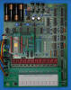
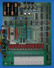
The DCM-50A (PLAYGROUND) supports the Characterization of the MK6010 Family single-chip calculator circuits using the DCM-50A Playground MK6010 Adapter mounted on top of the DCM-50A PG Digit Inverter Frame Carrier and supported by the DCM-50A PG KBD102 Keyboard configured to MK6010 Mode. The voltage selector jumper on the MK6010 Adapter must be set to the appropriate voltage. The optional DCM-50A Playground Digilent I/O Extender supports Characterization and Reverse-engineering of MK6010 Family single-chip calculator circuits.
 Device-under-Test:
| • Package Markings Top:
MOSTEK MK5010P C.747 7246KHI • Package Markings Bottom: • Donor Calculator: Rapid Data Rapidman 800, December 1972 |
Keyboard: The Rapid Data Rapidman 800 makes use of a basic Klixon™ 1KS108 keyboard array with 17 snap-action Klixon discs mounted on a printed circuit board for the interconnections of the switches to the external calculator circuit. The 17th switch contact is not used for the [CE] key of the MK5010 single-chip calculator circuit, but for the [ON/OFF] switch of the calculator. The 10 number keys are connected with a diode matrix to the key inputs KN1 to KN4 (Numbers) of the MK5010 while the 6 function keys are connected to its discrete key inputs with the [CE] key not connected. The Decimal Point selection is hardwired for two digits behind the decimal point with the DP1 input of the MK5010 connected to log.1 (VDD) and the DP2 input connected to log.0 (VSS).
Keyboard Matrix of the Rapid Data Rapidman 800:
MK5010 | ||||
| KEY | KN8 | KN4 | KN2 | KN1 |
| [1] | - | - | - | log.1 |
| [2] | - | - | log.1 | - |
| [3] | - | - | log.1 | log.1 |
| [4] | - | log.1 | - | - |
| [5] | - | log.1 | - | log.1 |
| [6] | - | log.1 | log.1 | - |
| [7] | - | log.1 | log.1 | log.1 |
| [8] | log.1 | - | - | - |
| [9] | log.1 | - | - | log.1 |
| [0] | log.1 | - | log.1 | - |
MK5010 | |||||||
| KEY | KC | KCE | KD | KM | KS | KAE | KP |
| [C] | log.1 | - | - | - | - | - | - |
| [÷] | - | - | log.1 | - | - | - | - |
| [×] | - | - | - | log.1 | - | - | - |
| [−] | - | - | - | - | log.1 | - | - |
| [+=] | - | - | - | - | - | log.1 | - |
| [.] | - | - | - | - | - | - | log.1 |
MK5010 | ||
| WIRE | DP2 | DP1 |
| [2] | - | log.1 |
 Display:
The Rapid Data Rapidman 800 makes use of a 9-digit LED display assembly composed of three Litronix DL-33 3-digit seven-segment LED displays housed in
12-pin packages and soldered onto
the double-sided Main-PCB. The Common Cathodes D1 to D8 of the LED display are connected with
eight PNP bipolar junction transistors (BJTs) to the Digit Outputs D1 to D8 of
the MK5010 while D9 is driven with its Sign Output. The A to G segments and
Decimal Point (Anodes) of the LED display are connected with eight PNP BJTs and
discrete current limiting 100 Ohm resistors to the Segment Outputs SA to SG and
SDP of the MK5010.
Display:
The Rapid Data Rapidman 800 makes use of a 9-digit LED display assembly composed of three Litronix DL-33 3-digit seven-segment LED displays housed in
12-pin packages and soldered onto
the double-sided Main-PCB. The Common Cathodes D1 to D8 of the LED display are connected with
eight PNP bipolar junction transistors (BJTs) to the Digit Outputs D1 to D8 of
the MK5010 while D9 is driven with its Sign Output. The A to G segments and
Decimal Point (Anodes) of the LED display are connected with eight PNP BJTs and
discrete current limiting 100 Ohm resistors to the Segment Outputs SA to SG and
SDP of the MK5010.
Display Layout:
| 3 Three-Digit LED Modules Litronix DL-33 |
 |
| The Segment drivers A-G and DP (Decimal Point) are connected to the 3 DL-33 displays in the pictured way. | 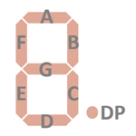 |
Display Fonts:
| Type | Calculator | Number Fonts | Decimal Separator |
Thousands Separator |
Entry Overflow |
Calculating Overflow |
Minus |
| MK5010 | Rapid Data Rapidman 800 |
 |
 |
n.a. |  |
|
 |

 Display
scanning: The MK5010 single-chip calculator circuit is manufactured in a
PMOS process and its Digit Scanning Outputs are high-side PMOS transistors. For
easy interfacing to low-voltage VFDs
(Vacuum Fluorescent Displays) or high-voltage
gas-discharge displays, an
activated digit corresponds to a logical 0 or open output. All other,
non-activated digits have the PMOS transistors turned on. Please notice that the
the DCM-50A PG Digit Inverter Frame Carrier used to characterize the MK5010 chip
is inverting the Digit Outputs D1 to D12 and we labeled them therefore /D1 to
/D12 on the graphs.
Display
scanning: The MK5010 single-chip calculator circuit is manufactured in a
PMOS process and its Digit Scanning Outputs are high-side PMOS transistors. For
easy interfacing to low-voltage VFDs
(Vacuum Fluorescent Displays) or high-voltage
gas-discharge displays, an
activated digit corresponds to a logical 0 or open output. All other,
non-activated digits have the PMOS transistors turned on. Please notice that the
the DCM-50A PG Digit Inverter Frame Carrier used to characterize the MK5010 chip
is inverting the Digit Outputs D1 to D12 and we labeled them therefore /D1 to
/D12 on the graphs.
Display scanning is performed in D1 → D12 direction at a rate of about 480 Hz:
|
• State Time = 0.5 Clocks = 0.020 ms @ CK=25 kHz • Digit Time = 8 States = 0.160 ms @ CK=25 kHz • Scan Time = 13 Digit Times (D1 to D13 with D13 a dead cycle) = 2.08 ms @ CK=25 kHz |
 Device-under-Test:
| • Package Markings Top:
MOSTEK MK5011P 7306KEG • Package Markings Bottom: • Donor Calculator: Unitrex 1200 (Type 37, Rev. 4C), May 1973 |
Keyboard: The Unitrex 1200 makes use of a keyboard assembly with 17 spring-loaded plastic keys pushing two fingers of stamped sheet-metal pieces soldered perpendicular on a single-sided phenolic PCB together. The 10 number keys are connected with a diode matrix to the key inputs KN1 to KN4 (Numbers) of the MK5011 while the 7 function keys are connected to its discrete key inputs. The 4-position sliding switch for the Decimal Point selection is connected with a diode matrix to the DP1 and DP2 inputs of the MK5011.
Keyboard Matrix of the Unitrex 1200 (Type 37, Rev. 4C):
MK5011 | ||||
| KEY | KN8 | KN4 | KN2 | KN1 |
| [1] | - | - | - | log.1 |
| [2] | - | - | log.1 | - |
| [3] | - | - | log.1 | log.1 |
| [4] | - | log.1 | - | - |
| [5] | - | log.1 | - | log.1 |
| [6] | - | log.1 | log.1 | - |
| [7] | - | log.1 | log.1 | log.1 |
| [8] | log.1 | - | - | - |
| [9] | log.1 | - | - | log.1 |
| [0] | log.1 | - | log.1 | - |
MK5011 | |||||||
| KEY | KC | KCE | KD | KM | KS | KAE | KP |
| [C] | log.1 | - | - | - | - | - | - |
| [CE] | - | log.1 | - | - | - | - | - |
| [÷] | - | - | log.1 | - | - | - | - |
| [×] | - | - | - | log.1 | - | - | - |
| [−] | - | - | - | - | log.1 | - | - |
| [+=] | - | - | - | - | - | log.1 | - |
| [.] | - | - | - | - | - | - | log.1 |
MK5011 | ||
| SWITCH | DP2 | DP1 |
| [4-3-2-0] | - | - |
| [4-3-2-0] | - | log.1 |
| [4-3-2-0] | log.1 | - |
| [4-3-2-0] | log.1 | log.1 |
 Display:
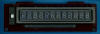
The Unitrex 1200 makes use of a Japan Radio Corporation (JRC) Septanix J4962E Planar Neon Gas Discharge
Display (Panaplex-style) connected with two Kyodo KH-6225 Digit Driver
Modules and 12 high-voltage capacitors as level shifters to the twelve Digit
Outputs D1 to D12 of the MK5011 and one Kyodo KH-6259 Segment Driver Module
connected to the Segment Outputs SA to SG and SDP of the MK5011. The display is
operated with approximately +180 Volts. An additional discrete orange miniature
gas-discharge lamp
is used as minus sign for negative numbers and connected with a transistor to
the Sign output of the MK5011.
Display:
The Unitrex 1200 makes use of a Japan Radio Corporation (JRC) Septanix J4962E Planar Neon Gas Discharge
Display (Panaplex-style) connected with two Kyodo KH-6225 Digit Driver
Modules and 12 high-voltage capacitors as level shifters to the twelve Digit
Outputs D1 to D12 of the MK5011 and one Kyodo KH-6259 Segment Driver Module
connected to the Segment Outputs SA to SG and SDP of the MK5011. The display is
operated with approximately +180 Volts. An additional discrete orange miniature
gas-discharge lamp
is used as minus sign for negative numbers and connected with a transistor to
the Sign output of the MK5011.
Display Layout:
| JRC Septanix J4962E plus Lamp |
 |
| The Segment drivers A-G and DP (Decimal Point) are connected to the JRC Septanix J4962E display in the pictured way. | |
Display Fonts:
| Type | Calculator | Number Fonts | Decimal Separator |
Thousands Separator |
Entry Overflow |
Calculating Overflow |
Minus |
| MK5011 | Unitrex 1200 (Type 37) |
|
|
n.a. |  |
|
 |
 Display
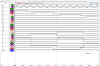
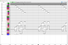
scanning: The MK5011 single-chip calculator circuit is manufactured in a
PMOS process and its Digit Scanning Outputs are high-side PMOS transistors. For
easy interfacing to low-voltage VFDs
(Vacuum Fluorescent Displays) or high-voltage
gas-discharge displays, an
activated digit corresponds to a logical 0 or open output. All other,
non-activated digits have the PMOS transistors turned on. Please notice that the
the DCM-50A PG Digit Inverter Frame Carrier used to characterize the MK5011 chip
is inverting the Digit Outputs D1 to D12 and we labeled them therefore /D1 to
/D12 on the graphs.
Display
scanning: The MK5011 single-chip calculator circuit is manufactured in a
PMOS process and its Digit Scanning Outputs are high-side PMOS transistors. For
easy interfacing to low-voltage VFDs
(Vacuum Fluorescent Displays) or high-voltage
gas-discharge displays, an
activated digit corresponds to a logical 0 or open output. All other,
non-activated digits have the PMOS transistors turned on. Please notice that the
the DCM-50A PG Digit Inverter Frame Carrier used to characterize the MK5011 chip
is inverting the Digit Outputs D1 to D12 and we labeled them therefore /D1 to
/D12 on the graphs.
Display scanning is performed in D1 → D12 direction at a rate of about 480 Hz:
|
• State Time = 0.5 Clocks = 0.020 ms @ CK=25 kHz • Digit Time = 8 States = 0.160 ms @ CK=25 kHz • Scan Time = 13 Digit Times (D1 to D13 with D13 a dead cycle) = 2.08 ms @ CK=25 kHz |

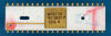 Device-under-Test:
| • Package Markings Top:
MOSTEK MK5012P 7246 B • Package Markings Bottom: • Donor Calculator: Caltronic 912, February 1973 |
Keyboard: The Caltronic 912 makes use of a Klixon™ 1KS116 keyboard assembly consisting of the "Basic 1KS" keyboard array with 17 snap-action Klixon discs mounted on a printed circuit board for the interconnections of the switches to the external calculator circuit and a stainless steel mounting frame and the molded keytops. In addition, the keyboard assembly integrates two two-position slide switches: one for selecting the decimal-point position and the other for switching the calculator power on and off. The 10 number keys are connected with a diode matrix to the key inputs KN1 to KN4 (Numbers) of the MK5012 while the 7 function keys are connected to its discrete key inputs. The 2-position sliding switch for the Decimal Point selection is connected with a diode matrix to the DP1 input of the MK5012 with the DP2 input connected to log.0 (VSS).
Keyboard Matrix of the Caltronic 912:
MK5012 | ||||
| KEY | KN8 | KN4 | KN2 | KN1 |
| [1] | - | - | - | log.1 |
| [2] | - | - | log.1 | - |
| [3] | - | - | log.1 | log.1 |
| [4] | - | log.1 | - | - |
| [5] | - | log.1 | - | log.1 |
| [6] | - | log.1 | log.1 | - |
| [7] | - | log.1 | log.1 | log.1 |
| [8] | log.1 | - | - | - |
| [9] | log.1 | - | - | log.1 |
| [0] | log.1 | - | log.1 | - |
MK5012 | |||||||
| KEY | KC | KCE | KD | KM | KS | KAE | KP |
| [C] | log.1 | - | - | - | - | - | - |
| [CE] | - | log.1 | - | - | - | - | - |
| [÷] | - | - | log.1 | - | - | - | - |
| [×] | - | - | - | log.1 | - | - | - |
| [−] | - | - | - | - | log.1 | - | - |
| [+=] | - | - | - | - | - | log.1 | - |
| [.] | - | - | - | - | - | - | log.1 |
MK5012 | ||
| SWITCH | DP2 | DP1 |
| [2-0] | - | - |
| [2-0] | - | log.1 |
 Display:
The Caltronic 912 makes use of a 9-digit LED display assembly composed of three Litronix DL-33 3-digit seven-segment LED displays housed in
12-pin packages and soldered onto
the double-sided Display-PCB. In addition to the numeric displays, the Display-PCB incorporates
an indicator LEDs for low-battery status. The
Display-PCB is connected to the Main-PCB of the Caltronic 912 with 21 hand-soldered
short wires. The Common Cathodes D1 to D8 of the LED display are connected with
eight PNP bipolar junction transistors (BJTs) to the Digit Outputs D1 to D8 of
the MK5012 while D9 is driven with its Sign Output. The A to G segments and
Decimal Point (Anodes) of the LED display are connected with eight PNP BJTs and
discrete current limiting 100 Ohm resistors to the Segment Outputs SA to SG and
SDP of the MK5012. The indicator for a low battery is controlled by the power
supply circuitry of the calculator.
Display:
The Caltronic 912 makes use of a 9-digit LED display assembly composed of three Litronix DL-33 3-digit seven-segment LED displays housed in
12-pin packages and soldered onto
the double-sided Display-PCB. In addition to the numeric displays, the Display-PCB incorporates
an indicator LEDs for low-battery status. The
Display-PCB is connected to the Main-PCB of the Caltronic 912 with 21 hand-soldered
short wires. The Common Cathodes D1 to D8 of the LED display are connected with
eight PNP bipolar junction transistors (BJTs) to the Digit Outputs D1 to D8 of
the MK5012 while D9 is driven with its Sign Output. The A to G segments and
Decimal Point (Anodes) of the LED display are connected with eight PNP BJTs and
discrete current limiting 100 Ohm resistors to the Segment Outputs SA to SG and
SDP of the MK5012. The indicator for a low battery is controlled by the power
supply circuitry of the calculator.
Display Layout:
| 3 Three-Digit LED Modules Litronix DL-33 |
|
|
| The Segment drivers A-G and DP (Decimal Point) are connected to the 3 DL-33 displays in the pictured way. | |
Display Fonts:
| Type | Calculator | Number Fonts | Decimal Separator |
Thousands Separator |
Entry Overflow |
Calculating Overflow |
Minus |
| MK5012 | Caltronic 912 |
|
|
n.a. | |
|
|
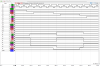
 Display
scanning: The MK5012 single-chip calculator circuit is manufactured in a
PMOS process and its Digit Scanning Outputs are high-side PMOS transistors. For
easy interfacing to low-voltage VFDs
(Vacuum Fluorescent Displays) or high-voltage
gas-discharge displays, an
activated digit corresponds to a logical 0 or open output. All other,
non-activated digits have the PMOS transistors turned on. Please notice that the
the DCM-50A PG Digit Inverter Frame Carrier used to characterize the MK5012 chip
is inverting the Digit Outputs D1 to D12 and we labeled them therefore /D1 to
/D12 on the graphs.
Display
scanning: The MK5012 single-chip calculator circuit is manufactured in a
PMOS process and its Digit Scanning Outputs are high-side PMOS transistors. For
easy interfacing to low-voltage VFDs
(Vacuum Fluorescent Displays) or high-voltage
gas-discharge displays, an
activated digit corresponds to a logical 0 or open output. All other,
non-activated digits have the PMOS transistors turned on. Please notice that the
the DCM-50A PG Digit Inverter Frame Carrier used to characterize the MK5012 chip
is inverting the Digit Outputs D1 to D12 and we labeled them therefore /D1 to
/D12 on the graphs.
Display scanning is performed in D1 → D12 direction at a rate of about 480 Hz:
|
• State Time = 0.5 Clocks = 0.020 ms @ CK=25 kHz • Digit Time = 8 States = 0.160 ms @ CK=25 kHz • Scan Time = 13 Digit Times (D1 to D13 with D13 a dead cycle) = 2.08 ms @ CK=25 kHz |

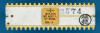 Device-under-Test:
| • Package Markings Top:
NCM MOSTEK MK6010 L QP-3550L 7206 B 2574 • Package Markings Bottom: • Donor Calculator: Busicom "HANDY-LE" LE-120S, March 1972 |
Keyboard: The Busicom LE-120S makes use of a keyboard assembly with 17 plastic keys pushing individual metal fingers soldered on a double-sided PCB against large, gold-plated contacts mounted on the PCB and a 3-position sliding switch to select the position of the decimal point. The 10 number keys are connected with a diode matrix to the key inputs KN1 to KN4 (Numbers) of the MK6010L while the 7 function keys are connected to its discrete key inputs. The 3-position sliding switch for the Decimal Point selection is connected with a diode matrix to the DP1 and DP2 inputs of the MK6010L.
Keyboard Matrix of the Busicom LE-120S:
MK6010L | ||||
| KEY | KN8 | KN4 | KN2 | KN1 |
| [1] | - | - | - | log.1 |
| [2] | - | - | log.1 | - |
| [3] | - | - | log.1 | log.1 |
| [4] | - | log.1 | - | - |
| [5] | - | log.1 | - | log.1 |
| [6] | - | log.1 | log.1 | - |
| [7] | - | log.1 | log.1 | log.1 |
| [8] | log.1 | - | - | - |
| [9] | log.1 | - | - | log.1 |
| [0] | log.1 | - | log.1 | - |
MK6010L | |||||||
| KEY | KC | KCE | KD | KM | KS | KAE | KP |
| [C] | log.1 | - | - | - | - | - | - |
| [CE] | - | log.1 | - | - | - | - | - |
| [÷] | - | - | log.1 | - | - | - | - |
| [×] | - | - | - | log.1 | - | - | - |
| [−] | - | - | - | - | log.1 | - | - |
| [+=] | - | - | - | - | - | log.1 | - |
| [.] | - | - | - | - | - | - | log.1 |
MK6010L | ||
| SWITCH | DP2 | DP1 |
| [4-2-0] | - | - |
| [4-2-0] | - | log.1 |
| [4-2-0] | log.1 | log.1 |
 Display:
The Busicom LE-120S makes use of a 12-digit LED display assembly composed of
twelve Monsanto MAN-3A seven-segment LED displays and two indicator LEDs for
negative values and low-battery status connected with twelve PNP bipolar
junction transistors (BJTs) to the twelve Digit
Outputs D1 to D12 of the MK6010L and eight PNP BJTs
connected with eight current limiting resistors to the Segment Outputs SA to SG and SDP of the MK6010L. An additional discrete
red LED
is used as minus sign for negative numbers and connected with a transistor to
the Sign output of the MK6010L while the indicator for a low battery is
controlled by the power supply circuitry of the calculator.
Display:
The Busicom LE-120S makes use of a 12-digit LED display assembly composed of
twelve Monsanto MAN-3A seven-segment LED displays and two indicator LEDs for
negative values and low-battery status connected with twelve PNP bipolar
junction transistors (BJTs) to the twelve Digit
Outputs D1 to D12 of the MK6010L and eight PNP BJTs
connected with eight current limiting resistors to the Segment Outputs SA to SG and SDP of the MK6010L. An additional discrete
red LED
is used as minus sign for negative numbers and connected with a transistor to
the Sign output of the MK6010L while the indicator for a low battery is
controlled by the power supply circuitry of the calculator.
Display Layout:
| Busicom QP-3731 plus LED |
 |
| The Segment drivers A-G and DP (Decimal Point) are connected to the Busicom QP-3731 display in the pictured way. | |
Display Fonts:
| Type | Calculator | Number Fonts | Decimal Separator |
Thousands Separator |
Entry Overflow |
Calculating Overflow |
Minus |
| MK6010L | Busicom LE-120S |
|
|
n.a. | |
|
|
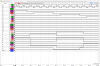
 Display
scanning: The MK6010L single-chip calculator circuit is manufactured in a
PMOS process and its Digit Scanning Outputs are high-side PMOS transistors. For
easy interfacing to low-voltage VFDs
(Vacuum Fluorescent Displays) or high-voltage
gas-discharge displays, an
activated digit corresponds to a logical 0 or open output. All other,
non-activated digits have the PMOS transistors turned on. Please notice that the
the DCM-50A PG Digit Inverter Frame Carrier used to characterize the MK6010L chip
is inverting the Digit Outputs D1 to D12 and we labeled them therefore /D1 to
/D12 on the graphs.
Display
scanning: The MK6010L single-chip calculator circuit is manufactured in a
PMOS process and its Digit Scanning Outputs are high-side PMOS transistors. For
easy interfacing to low-voltage VFDs
(Vacuum Fluorescent Displays) or high-voltage
gas-discharge displays, an
activated digit corresponds to a logical 0 or open output. All other,
non-activated digits have the PMOS transistors turned on. Please notice that the
the DCM-50A PG Digit Inverter Frame Carrier used to characterize the MK6010L chip
is inverting the Digit Outputs D1 to D12 and we labeled them therefore /D1 to
/D12 on the graphs.
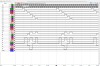
Display scanning is performed in D1 → D12 direction at a rate of about 480 Hz:
|
• State Time = 0.5 Clocks = 0.020 ms @ CK=25 kHz • Digit Time = 8 States = 0.160 ms @ CK=25 kHz • Scan Time = 13 Digit Times (D1 to D13 with D13 a dead cycle) = 2.08 ms @ CK=25 kHz |

If you have additions to the above article please email: joerg@datamath.org.
© Joerg Woerner, March 22, 2026. No reprints without written permission.