DATAMATH CALCULATOR MUSEUM
|
DATAMATH CALCULATOR MUSEUM |
It must have been a shockwave for a handful of Japanese companies, when Texas Instruments demonstrated in 1967 with the Cal-Tech feasibility study for the first time the application of LSI (Large Scale Integration) chips for portable, battery-operated calculators. American companies not only invented the transistors and ICs (Integrated Circuits) used with electronic calculators in the second half of the 1960s, but they also had a lead in the design and manufacturing of chips using PMOS (p-channel Metal–oxide Semiconductor) technology. On the other hand, Japanese companies like Canon, Casio, Sanyo, Sharp and Toshiba almost completely owned in 1967 the market of electronic desktop calculators and successfully developed, manufactured and sold their products designed around transistors and ICs.
The major manufacturers of electronic desktop calculators acted swiftly and locked into relationships with chips manufacturers capable of designing and producing PMOS LSI devices. In a first wave, around 1969/1970, three successful results of these collaborations hit the market:
|
• October 1969 - Sharp
QT-8D, Rockwell Chipset • April 1970 - Canon Pocketronic, Texas Instruments Chipset • May 1970 - Sanyo ICC-82D, General Instrument Chipset |
The second wave of partnerships between Japanese desktop calculator manufacturers and American chip manufacturers can be identified with:
|
• Busicom 141-PF, Intel Chipset (Famous 4004 microprocessor) • Busicom Handy LE-120, Mostek Chip • Toshiba BC-1215/BC-1216P, American Microsystems, Inc. (AMI) Chipset |
The winning team in the race to the first "small electronic desktop calculator" was obviously Sharp with the QT-8D using a chipset of five devices jointly developed with North American Rockwell’s Autonetics division: NRD2256, AC2261, DC2266, AU2271 and the clock driver CG1121. Sharp reused this chipset with the ELSI-8 (EL-8), a compact, battery-operated calculator introduced in November 1970, its offspring ELSI-8A and the QT-8B variation of the QT-8D. An upgraded design of the Rockwell chipset supported a User Memory function deployed in the battery-operated EL-8M and the EL-160 small electronic desktop calculator.
The 1st Generation with four LSI chips and one MSI chip still used the "old-style" Rockwell device markings. The complexity of the chips approached 1,000 transistors, commonly known as the threshold for LSI (Large Scale Integration) ICs. In March 1969, Sharp reached an agreement for technological cooperation with North American Rockwell and made an official announcement on the construction of a semiconductor plant. Construction of the semiconductor plant, the Central Research Laboratories, was completed in September 1970. Initially the semiconductor plant in Tenri was working only on the second half of the manufacturing process. It imported LSI chip wafers from North American Rockwell and then placed those chips in packages and finished them as LSIs. In 1972, the plant started operation of the first-half processes and became a facility for complete manufacture of LSIs.
These chips are manufactured in a 15 um metal gate PMOS process with enhancement mode transistors used for both gates and loads and using Ceramic Quad In-line Packages (QIP) with 42 pins or a 10-pin Metal Header Package (TO-100).
| Type | Year | Function | Calculators | Comments |
| AC2261 | 1969 | Address Control Chip | Sharp QT-8D, Sharp QT-8B, Sharp EL-8, Sharp EL-8A, Addo-X 9354J, Burroughs C3155, Facit 1111 | Internal PIN: 10001 |
| AU2271 | Arithmetic Unit Chip | Internal PIN: 10002 | ||
| DC2266 | Decimal-point Control Chip | Internal PIN: 10003 | ||
| NRD2256 | Numeric Read-in and Display Chip | Internal PIN: 10004 | ||
| CG1121 | Clock Generator Chip | Internal PIN: 10005 | ||
| ACM1156 | 1970 | Address Control and Memory Chip | Sharp EL-8M, Sharp EL-160, Burroughs C3260 | |
| AU2271 | Arithmetic Unit Chip | Internal PIN: 10002 | ||
| DC1152 | Decimal-point Control Point Chip | |||
| NRD2256 | Numeric Read-in and Display Chip | Internal PIN: 10004 | ||
| CG1121 | Clock Generator Chip | Internal PIN: 10005 |
While these chips sport on their Ceramics or Metal can packages the above-mentioned device marking, are the silicon chips inside the packages marked with 1000x – hinting to the original Part Numbering System used with North American Rockwell’s Autonetics division: Sequential numbers for each design, starting with 10001.
The massive contract from Sharp, $30 million US$ in 1969 or around $250 million US$ inflation adjusted in 2025, was Rockwell’s entry into the MOS LSI business, but the contracts with Sharp covered only delivery of these chips till January 1971. Under an agreement between the two companies, Sharp would manufacture them as soon as in 1971 in Japan with technical assistance from Rockwell – jumpstarting Sharp’s entry as provider for MOS LSI Chips.
Rockwell on the other hand understood the opportunities of their PMOS LSI technology and experience to mass-produce chips very competitively for consumer electronics and started the design of their own "Standard Building-Block Circuits for Calculators". This set of modular building blocks consisted of four Standard Building Blocks that needed an additional customer-programmed MOS ROM (Read-only Memory) and interfacing logic for the Input (Keyboard) and Output (Display and/or Printer) Interfaces to complete the electronics of a desktop calculator. The architecture of the Building Blocks allowed even for printing or programmable desktop calculators with 10 to 16 digits of capacity and when the North American Rockwell Microelectronics Company announced on January 13, 1971 the chip set, they dreamed big.
The four Standard Building Blocks or Calculator Chips were nick-named C, A, T, and S based on their functionality:
The C Chip
The C chip serves as
master control over other chips in the standard calculator chipset, contains
status registers, senses the status of selected registers, the status of
flip-flops as selected by ROM address, and the status of keyboard inputs such as
the decimal point. Using this information, the C chip generates output commands
to coordinate the activities of the other calculator chips.
The A Chip
The A chip includes circuitry for input/output logic control of the data entered into various registers. Specifically, the A chip contains a serial decimal adder, a ROM address register, a two-level stack for return address storage, register status determining logic, X and Y register storage and shift logic, and operand inter-register transfer logic.
The T Chip
The T chip contains the arithmetic registers, the memory registers for four numbers (of length 10, 12, 14, or 16 decimal digits, depending upon the model) in four memory registers and interfacing logic to a keyboard.
The S Chip
The S chip contains logic for auxiliary register Z, exponents, and binary logic. It also contains the exponent register and the master time-base generator. Two hard-wired inputs to the S chip cause the time-base to generate clocking for word lengths of 10, 12, 14, or 16 digits.
ROM Circuits
The ROM circuitry is implementing the microprogram for the set of standard calculator chips. In addition, the ROM contains the 4-phase clock for the calculator.
The ROM is available with three different capacities – 256, 384, or 512 words of 17 bits, each. There may be as many as four micro instructions per word.
Input/Output Chips
Depending upon requirements of the particular calculator system, from one to four input/output interfacing chips are necessary.
Programmability
Additional dynamic storage is required for a programmable calculator. From one to three additional chips are needed for those storage, depending upon the lengths of the program (number of instructions) and the type of instructions which are to be implemented.
Register Expandability
A "TT" chip may be substituted for the T chip, and with the addition of one or two “M” chips either eight or sixteen independent full registers may be obtained.
Each M chip contains eight memory registers, including decimal point and sign of each word.
As of today, we discovered less than ten designs centered around the C-A-T-S Standard Building-Block Circuits for Calculators and typical designs make use of six or seven PMOS LSI chips. Coincidence or not, these designs look very, very similar to an earlier chipset with six PMOS LSI chips used in Sharp’s CS-363 and CS-242 desktop calculators, with observed Date codes as early as November 1970. We assume that "tit for tat" translated in 1970 into:
|
• Sharp’s access to Rockwell’s chip design and manufacturing knowhow • Rockwell’s access to Sharp’s calculator logic design knowhow |
Here at the Datamath Calculator Museum we differentiate between customer-specific and generic calculator chips and chipsets and separate in our overview the original Sharp chipset from the C-A-T-S chipset, accordingly.
These chips are manufactured in a 15 um metal gate PMOS process with enhancement mode transistors used for both gates and loads and using Plastic or Ceramic Quad In-line Packages (QIP) with 42 pins and metal lids.
| Type | Year | Function | Calculators | Comments |
| 10061 | 1970 | Sharp CS-363, Sharp CS-242, Facit 1137J | Only Sharp CS-363, Facit 1137J | |
| 10062 | ||||
| 10063 | ||||
| 10064 | ||||
| 10065 | ||||
| 10066 | ||||
| 10321 | 1970 | Sharp CS-242 | Replacement for 10061 |
We assume that the
C-A-T-S Standard Building Blocks are based on the
Second Rockwell Chipset produced for Sharp with the
Part Numbers 10061 - 10066.
These chips are manufactured in a 15 um metal
gate PMOS process with enhancement mode transistors used for both gates and
loads and using Plastic or Ceramic Quad In-line Packages (QIP) with 42 pins and
metal lids.
| Type | Year | Function | Calculators | Comments |
| 10177 | 1971 | C Chip | Victor 18-1721, 18-1441, 18-3440, 18-3441 Anita 1211P, 1212D, 1233D Totalia LS14.1 Monroe 1350 |
|
| 10178 | A Chip | |||
| 10179 | T Chip | |||
| 10180 | S Chip | |||
| 10182 | 1971 | Input/Output Chip | Victor 18-1721, 18-1441 | |
| 10306 10307 |
1971 | Input/Output Chip | Victor 18-3440, 18-3441 | Printer |
| 10363 | 1971 | Input/Output Chip | Anita 1211P | Printer |
| 10560 | 1971 | Input/Output Chip | Totalia LS14.1 | Printer |
| 10562 | 1971 | Input/Output Chip | Anita 1212D, 1233D | |
| 10564 | 1972 | Input/Output Chip | Monroe 1350 | 14-digit Display |
| 10565 | 1972 | Input/Output Chip | Monroe 1350 | EP-102 Printer |
| 15000 | 1971 | ROM Chip | Victor 18-1441 | |
| 15003 | 1971 | ROM Chip | Anita 1212D, 1233D | |
| 15020 | 1971 | ROM Chip | Victor 18-3441 | |
| 15022 | 1971 | ROM Chip | Totalia LS14.1 | |
| 15023 | 1971 | ROM Chip | Anita 1211P | |
| 15027 | 1971 | ROM Chip | Victor 18-3440 | |
| 15170 | 1972 | ROM Chip | Monroe 1350 | |
| 15320 | 1971 | ROM Chip | Victor 18-1721 |
The 3rd Generation introduced end of
1971 combined the same functionality into just two LSI chips. Starting 1972,
Sharp manufactured these chips under license from Rockwell in their Tenri
semiconductor plant.
These chips are manufactured in a 10 um metal gate
PMOS process with enhancement mode transistors used for both gates and loads and using
Plastic Quad In-line Packages (QIP) with 42 pins and metal lids.
| Type | Year | Function | Calculators | Comments |
| 10572 | 1971 | TBD Chip | Sharp EL-811, Prinztronic MC85 | |
| 10573 | TBD Chip | |||
| 10580 | 1972 | TBD Chip | Sharp EL-811A, Commodore M16, Prinztronic MC95 | |
| 10631 | TBD Chip |
We assume that the these chips are based on the
Third Rockwell Chipset produced for Sharp with the
Part Numbers 10572 and 10573.
These chips are manufactured in a 15 um metal
gate PMOS process with enhancement mode transistors used for both gates and
loads and using Plastic Quad In-line Packages (QIP) with 42 pins and metal lids.
| Type | Year | Function | Calculators | Comments |
| 10567 | 1972 | TBD Chip | Victor 19-1421, Victor MEC2 | |
| 10584 | TBD Chip |
North American Rockwell pioneered the development
of Liquid-Crystal Displays (LCDs) and introduced already in 1972 "almost" single-chip
calculator circuits using external display drivers and LCD modules. Rockwell
manufactured with these components calculators for various OEMs like Lloyd's,
Rapid Data and Sears. Rockwell changed their Part Numbering
System in Fall 1972 and used 15xxx numbers for ROMs (Read-only Memorys) and
devices integrating ROM-structures. ROM-based calculator chips were consequently
renamed from 10xxx to 15xxx numbers.
These chips are manufactured in a 10 um metal
gate PMOS process with enhancement mode transistors used for both gates and
loads and using Plastic Quad In-line Packages (QIP) with 42 pins and metal lids.
| Type | Year | Function | Calculators | Comments |
| 10362 | 1972 | Main Chip | Lloyd's Accumatic 100 | Uses external LSI Display Drivers |
| 10661 | 1972 | Main Chip | Rapidman 1208LC, Sears 801.58000 | Uses external LSI Display Drivers |
| 15310 | 1972 | Main Chip | Lloyd's Accumatic 70 | Uses external LSI Display Drivers |
| 15311 | 1972 | Main Chip | Lloyd's Accumatic 70, Rapidman 1208LC, Unifive 1000 | Uses external LSI Display Drivers |
| 15361 | 1973 | Main Chip | Sears 801.58040 | Uses external LSI Display Drivers |
| 10417 | 1973 | LCD Segment Driver Chip | All Desktop Calculators with LC-Dislay | 33 Outputs for 4 7-Segment Digits with Decimal Point and Sign |
Work-In-Progress.
Work-In-Progress.
Rockwell introduced in 1973 with the 15330 -
later renamed to A1030 and even later to A4130 - their first single-chip
calculator circuit. The architecture of the 15330 is very similar to Rockwell's
PPS-4 (short for Parallel Processing System, 4-bit) system. The development of
this groundbreaking calculator chip prepared the design of the later
PPS-4/1 (short for Parallel Processing System, 4-bit, Single-chip) system, a
Digit Processor
competing directly with the Texas Instruments TMS1000
Microcomputer introduced in October 1974. The programmable ROM (Read-Only
Memory) of the 15330 is with 512 x 8 Bits capacity much smaller than the TMS1000
ROM with its 1,024 x 8 Bits capacity, while the RAM with 48 x 4 Bits is almost
on par with the TMS1000 sporting 64 x 4 Bits.
The 15330 and its derivatives 15332, 15334 and 15336 (aka A1032, A1034
and A1036) are manufactured in a 10 um metal gate
PMOS process with enhancement mode transistors used for both gates and loads and using
Plastic Quad In-line Packages (QIP) with 42 pins and metal lids.
| Type | Year | Function | Calculators | Comments |
| 15330/A1030/A4130 | 1973 | Basic | Anita 811, Kovac SM-818M, Toshiba BC-0811B, Triumph-Adler 81, Unicom 103 | [+] [−] [=] keys, MD Constant, Memory
with AM, Rounding, %, 8 digits Adding Machine Logic |
Work-In-Progress.
Rockwell introduced in June 1974 with the A5300
Product Family the first single-chip calculator circuits with LED
(Light-Emitting-Diode) Direct-Drive capability. Earlier chip designs, like Texas
Instruments' TMS0100
Product Family, lacked any display drivers and left the choice of display
technology and the associated drivers to their customers. Both improvements of
the efficiency of LEDs and the design of beefier output drivers allowed at least
omitting the Segment Drivers starting around 1973 with designs like the Rockwell
15330. Looking closely into the A5300 reveals a design very similar to
Rockwell's PPS-4/1 (short for Parallel Processing System, 4-bit,
Single-chip) system, a
Digit Processor
competing directly with the Texas Instruments TMS1000
Microcomputer introduced in October 1974. The programmable ROM (Read-Only
Memory) of the A5300 is with 504 x 8 Bits capacity much smaller than the TMS1000
ROM with its 1,024 x 8 Bits capacity, while the RAM with 48 x 4 Bits is almost
on par with the TMS1000 sporting 64 x 4 Bits. As a result is the die size of the
A5300 with around 4.0 mm x 3.8 mm significantly smaller than the TMS1000 which
measures about 5.1 mm x 5.1 mm. The CPU architecture of the PPS-4/1 was designed
with electronic calculators in mind and consequently were the software engineers
able to squeeze a fully-featured five-function calculator with Memory into the
small program memory of the A5300.
The A5300 is manufactured in an 8 um metal
gate PMOS process with enhancement mode transistors used for both gates and
loads and using Plastic Quad In-line Packages (QIP) with 42 pins and metal lid.
| Type | Year | Function | Calculators | Comments |
| A5300 | 1974 | Basic | APF Mark 26, Rockwell 20R | [+] [−] [=] keys, MDAS Constant, 6-function Memory, %, 8 digits Chain Logic |
Work-In-Progress.
Work-In-Progress.
The numbering scheme used to mark Integrated Circuits manufactured by North American Rockwell changed multiple times and here at the Datamath Calculator Museum we focus on the timeframe between 1969 and about 1979, the peak of Rockwell's engagement in supplying MOS LSI (Metal-oxide Semiconductor Large Scale Integration) chips for electronic calculators.
Part numbering of Integrated Circuits is a complex topic, and one needs to look into it under different angles. The package of the housing contains one set of information while the silicon die inside the encapsulations holds another set of information. The package, both its top and bottom sides typically bear a manufacturer identification, product identification number, device revision, manufacturing date, manufacturing/packaging site, temperature rating, speed rating, and more. None of this labeling information is standardized and most companies create their own coding scheme. Just with MOS LSI calculator chips, Rockwell changed their part numbering at least twice within three years…
The silicon die itself contains markings from its photomasks that reference to the underlying schematics of the chip, its layout artwork, revision/process version and other information. Usually, this information is encrypted in just a few letters and numbers, real estate on silicon dies is precious.
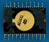
When North American Rockwell’s Autonetics division surprised in 1969 the industry with the famous Chipset for Sharp's groundbreaking QT-8D and EL-8 calculators, they simply named the five devices on the silicon die with sequential numbers 10001 to 10005. The package chips on the other hand were named NRD2256, AC2261, DC2266, AU2271, CG1121 – with the characters hinting to the functionality of the respective chips, NRD2256 as an example refers to the "Numeric Read-in and Display" Building Block of the calculator brain while the meaning of 2256 is not yet understood. Being an exclusive custom design for Sharp, Rockwell had to mark the packages per Sharp's request. Additionally have these earliest Rockwell chips only a 4-digit Date Code and a small Rockwell logo printed on the metal cap of the 42-pin Quad-In-Line ceramics package. The silicon die of the NRD2256 chip identifies simply as 10001.
Rockwell kept the sequential product identification numbering scheme of MOS LSI chips for some time and the number itself gives a good understanding of the timeframe of the chip development. Some examples to illustrate this idea are the first generation of the "C-A-T-S Standard Building-Block Circuits for Calculators" introduced in October 1970 and using the numbers 10061 to 10066, the second generation introduced in Spring 1971 and using 10177 to 10182 and the first chipset for LCD calculators introduced in Summer 1972 (10362).
With the second generation of the C-A-T-S Building Blocks, Rockwell introduced a change of the product identification numbering system and marked ROM (Read-only Memory) devices with numbers starting with 15000 and most other chips with a programmable ROM defining its functionality like Rockwell's early 15332 single-chip calculator circuit adopted the 15xxx product identification numbering. With the introduction of the PPS-4 in Fall 1972, Rockwell changed the product identification numbering of ROM devices again, using a leading “A” character before the number. While the PPS-4 CPU was simply called 10060 and its RAM chip was marked 10532, used the initially available ROM devices A05xx product identification number markings. Rockwell adopted this scheme to some calculator chips, too and the above mentioned 15332 chip was renamed mid of 1973 to A1032 and the 15350 single-chip calculator circuit for example was marked as A1150. During a transition time, the chips used both markings to avoid/create confusion.
These changes are clearly a sign of Product Managers and Marketing Managers having now the responsibility for device marking and not the R&D Teams anymore. In the pursuit to have the best numbering scheme, Rockwell changed the nomenclature for calculator chips with the introduction of the A4800 single-chip calculator circuit again and renamed the 15470 chips to A4000 and the 15350/A1150 to A4350 – finally going from "early designs = low 10xxx numbers" to "high functionality = high A4xxx numbers". The power of marketing.
A typical Rockwell calculator chip sold in Spring 1973 would have these markings on the metal cap of its housing:
15330PC
7312
Rockwell logo
| • In this example 15330 would
refer to a single-chip calculator circuit with 8-digit capability and
ROM Version "0" • The character P to the right of the number would indicate a 42-pin QIP (Quad In-line Package) and the character C refers to the third revision of the chip design • The four digit number 7312 is the Date code and translates into a packaging/testing date of week 12, in the year 1973 |
The same calculator chip sold in Fall 1973 would read:
15330
A1030PD
7341
Rockwell logo
And in 1976 the very same chip showed up in a Rockwell 330 calculator with the markings:
15330
A4130CA
7629
Rockwell logo
And in this case the chips are using the same 42-pin QIP (Quad In-line Package), its package code was changed over the course of time from "P" to "C".
In the past years we assembled a list of Rockwell package markings located on early Standard Building Blocks for calculators, single chip calculator circuits, PPS-4, PPS-4/2 and PPS-4/1 devices and single-chip designs for electronic toys – trying to reverse-engineer the logic behind the numbering scheme used in the 1970s for MOS LSI devices. Please find below a summary of our understanding of Rockwell’s early MOS LSI device marking codes as of today and don’t hesitate to get in touch with us with your valuable insights. Thank you.
Early North American Rockwell's LSI (Large Scale Integration) chips using PMOS (p-channel Metal–oxide Semiconductor) technology are using three markings on top of the chip packaging:
PxxxxYZ Product Identification (...1974)
yyww Date code
Rockwell logo Manufacturer Identification
The Product Identification Number xxxx is a unique part number for each device, the Package Type is encoded in a single character Y following the part number and the Photomask Revision is encoded in a second character Z. The leading letter or number P refers to the Process Technology of the chip.
Starting in 1974, North American Rockwell used the first digit of the Product Identification Number to encode the Product Category
c and the second character for the Product Family f:
PcfxxYZ Product Identification (1974...1978)
North American Rockwell Product Category changed in 1978 the coding of the Product Identification slightly, omitting the Package Type and introducing a Temperature Range
t marking, separated by a
"-" and switching the Photomask Revision from letters Z to numbers
z:
Pcfxx-tz Product Identification (1978...)
Process Technology (P):
|
• 1 First and early generation of pMOS processes, usually between 15 volts and 25 volts supply • A Later pMOS processes, typically 15 volts supply. Devices with on-chip ROM (Read-only Memory) • B Final pMOS process, typically 9 volts supply. Devices with on-chip ROM (Read-only Memory) |
Product Identification Number (xxxx):
The Product Identification Number xxxx went over the course of the 1970s through four iterations:
|
• Sequential numbers, starting with 0001 – Introduced with the first commercial PMOS LSI devices in 1969 • Sequential numbers, starting with 5000 for devices with on-chip ROM (Read-only Memory) – Introduced with the second generation of the C-A-T-S Building Blocks in 1971 • Related numbers, e.g. 10432 for 256x4 bits RAM and 10932 for 512x4 Bits RAM or 10660 for CPU, 10760 for its clock generator and 12660 for CPU with integrated clock generator – Introduced with PPS-4 Product Family in 1972 • Block numbers, e.g. A40xx and A48xx for two families of single-chip calculator circuits with 15 volts supply and no integrated LED digit drivers– Introduced in 1974 |
Package Type for Quad In-line Packages (Y):
|
• N 42-pin QIP, white ceramics, golden lid, golden chip carrier • P 42-pin QIP package, grey plastics, metal lid, metal chip carrier (...1976) • C 42-pin QIP package, grey plastics, metal lid, metal chip carrier (1976...) • E 42-pin QIP package, grey plastics, no lid (1977...) |
Photomask Revision (Z,z):
|
• A Original Mask set (...1978) • B Revision 1 (...1978) • C Revision 2 etc. (...1978) • 1 Original Mask set (1978...) • 2 Revision 1 (1978...) • 3 Revision 2 etc. (1978...) |
| • _ 0°C to +70°C (Commercial Grade) • 1 0°C to +50°C (Consumer Grade) • 2 -40°C to +85°C (Industrial Grade) |
| • 4, 5 Electronic Calculators • 6 Electronic Games • 7, 8, 9 PPS-4/1 Product Family |
Note: The Product Category numbering scheme has some exclusions due to grandfathering Axxxx numbers from the PPS-4 Product Families and renaming of early calculator chips from their 15xxx to Axxxx numbers. We identified as of today:
|
• A05xx PPS-4 1024 x 8 Bits ROM • A07xx PPS-4 1024 x 8 Bits ROM / 116 x 4 Bits RAM • A08xx PPS-4 704 x 8 Bits ROM / 72 x 4 Bits RAM • A103x Renamed 1533x Calculator Chips • A115x Renamed 1535x Calculator Chips • A12xx Calculator Chips renamed to A46xx • A17xx PPS-4/2 2048 x 8 Bits ROM / 128 x 4 Bits RAM / 16 IO lines • A20xx PPS-4/2 1536 x 8 Bits ROM / 128 x 4 Bits RAM • A21xx PPS-8/2 2048 x 8 Bits ROM / 64 x 8 Bits RAM • A22xx PPS-8/2 1024 x 8 Bits ROM / 64 x 8 Bits RAM • A23xx PPS-4/2 1024 x 8 Bits ROM / 128 x 4 Bits RAM / 16 IO lines • A52xx PPS-4 2048 x 8 Bits • A66xx PPS-4 4096 x 8 Bits • A88xx PPS-4 8192 x 8 Bits |
Electronic Calculators:
|
• A400x Renamed 1547x Chips, 1056 x 8 Bits ROM, 96 x 4 Bits RAM, 8 Digits • A406x tbd • A408x tbd • A413x Renamed A103x/1533x Chips • A42xx Printing Calculators • A435x Renamed A115x/1535x Chips • A44xx tbd • A45xx tbd • A46xx Renamed A12xx Chips, 640 x 8 Bits ROM, 64 x 4 Bits RAM, 8 Digits • A48xx 1536 x 8 Bits ROM, 96 x 4 Bits RAM, 12 Digits • A49xx Printing Calculators • A50xx 448 x 8 Bits ROM, 45 x 4 Bits RAM, 8 Digits, LED Direct-Drive • A53xx 504 x 8 Bits ROM, 48 x 4 Bits RAM, 8 Digits, LED Direct-Drive • A546x 8 Digits • A55xx 768 x 8 Bits ROM, 48 x 4 Bits RAM, 8 Digits, LED Direct-Drive • A56xx tbd • A57xx Printing Calculators • A56xx tbd • A59xx 512 x 8 Bits ROM, 45 x 4 Bits RAM, 8 Digits, LED Direct-Drive • B50xx 448 x 8 Bits ROM, 45 x 4 Bits RAM, 8 Digits, LED Direct-Drive • B55xx 768 x 8 Bits ROM, 48 x 4 Bits RAM, 8 Digits, LED Direct-Drive |
Misfits:
|
• A640x Printing Calculators • A650x 8 Digits |
Electronic Games:
|
• B60xx Based on B50xx, 512 x 8 Bits ROM, 45 x 4 Bits RAM, 8 Digits, LED Direct-Drive, Buzzer • B61xx Based on B51xx, 896 x 8 Bits ROM, 48 x 4 Bits RAM, 8 Digits, LED Direct-Drive, Buzzer |
PPS-4/1 Product Family:
|
• A75xx PPS-4/1 MM75 640 x 8 Bits ROM / 48 x 4 Bits RAM / 22 IOs / 15 Volts / DIP-28 • A76xx PPS-4/1 MM76 640 x 8 Bits ROM / 48 x 4 Bits RAM / 31 IOs / 15 Volts / QIP-42 • A77xx PPS-4/1 MM77 1344 x 8 Bits ROM / 96 x 4 Bits RAM / 31 IOs / 15 Volts / QIP-42 • A78xx PPS-4/1 MM78 2048 x 8 Bits ROM / 128 x 4 Bits RAM / 31 IOs / 15 Volts / QIP-42 • A79xx PPS-4/1 MM76C 640 x 8 Bits ROM / 48 x 4 Bits RAM / 39 IOs / Counter / 15 Volts / QIP-52 • A86xx PPS-4/1 MM76E 1024 x 8 Bits ROM / 48 x 4 Bits RAM / 31 IOs / 15 Volts / QIP-42 • B76xx PPS-4/1 MM76L 640 x 8 Bits ROM / 48 x 4 Bits RAM / 31 IOs / 9 Volts / DIP-40 • B77xx PPS-4/1 MM77L 1344 x 8 Bits ROM / 96 x 4 Bits RAM / 31 IOs / 9 Volts / DIP-40 • B78xx PPS-4/1 MM78L 2048 x 8 Bits ROM / 128 x 4 Bits RAM / 31 IOs / 9 Volts / DIP-40 • B86xx PPS-4/1 MM76EL 1024 x 8 Bits ROM / 48 x 4 Bits RAM / 31 IOs / 9 Volts / DIP-40 • B90xx PPS-4 MM78LA/MM95 2048 x 8 Bits ROM / 128 x 4 Bits RAM / 35 IOs / Speaker / 9 Volts / QIP-42 |
| • 1969 - 15 um metal gate PMOS, enhancement mode transistors for gates and loads • 1971 - 10 um metal gate PMOS, enhancement mode transistors for gates and loads • 1973 - 8 um metal gate PMOS, enhancement mode transistors for gates, depletion mode transistors for loads |
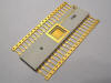
When Sharp introduced in October 1969 with the QT-8D the World's first small electronic desktop calculator, it was using a Chipset of five LSI (Large Scale Integration) Integrated Circuits jointly developed with North American Rockwell’s Autonetics division. Four of the five chips were packaged in 42-pin Quad In-line Packages (QIP) with their prominent staggered footprint. Rockwell stayed this at first glance unusual package committed for most, if not all, of its later calculator chips and due to a technology exchange with Sharp it quickly gained popularity in Japan. General Instrument / Sanyo adopted the package with a smaller pin count, NEC added a larger 64-pin variation and Rockwell added a 52-pin version to its portfolio. As of today we know variations of the QIP with 36 pins, 42 pins, 52 pins and 64 pins.
Rockwell introduced the 42-pin package in 1969 with a hermetically sealed white ceramic body, gold-finished bottom and top metal caps and gold plated pins. In 1972 the design was cost-optimized, using a 42-pin lead frame with tin plated pins, a grey plastic encapsulation and tops and bottom metal caps. In 1977 the final design was of the 42-pin QIP was introduced, omitting the metal caps of the housing and mimicking the setup of standard Dual In-line Packages (DIP). This style of plastic-encapsulated lead frames was introduced for DIP already in the 1960s and Texas Instruments used 28-pin and 40-pin DIP for calculator chips already in 1970, leading to the question:
| • Why did Rockwell utilize the rather expensive 42-pin QIPs with metal caps till 1977? |
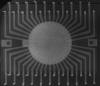
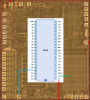
It is all about power distribution on the chip! Early calculator chips in the 1970s were manufactured in PMOS (p-Channel MOS) technology and the substrate of the small silicon dies needs to be connected to the most positive voltage, usually labeled VSS. The PMOS output transistors of these chips are "high-side" switching, meaning they conduct to VSS when activating a digit or segment output. In typical calculator applications, the output currents of one output are in the range between 1 mA (external digit and segment drivers) and about 5 mA to 10 mA (integrated segment drivers). When displaying an "8" with the decimal point lit, the output currents of the eight segment drivers might add up to around 50 mA, tenfold higher than the typical supply current of such a calculator chip.
![]() The semiconductor process technology of the 1970s
did allow for only one metal layer to route all the signals on the silicon chip and special care needed to be taken to connect the substrate
properly to VSS and distribute the VSS pin to all segment
driver output transistors. One neat trick in the toolbox of the team creating
the layout of the chip topology was using the exposed die paddle of the lead
frame as an additional layer to route the high-current VSS power
path. Looking for example at an overlay of the actual pin connection of the
TMS0850 single-chip calculator circuit and its
chip layout helps to explain this approach:
The semiconductor process technology of the 1970s
did allow for only one metal layer to route all the signals on the silicon chip and special care needed to be taken to connect the substrate
properly to VSS and distribute the VSS pin to all segment
driver output transistors. One neat trick in the toolbox of the team creating
the layout of the chip topology was using the exposed die paddle of the lead
frame as an additional layer to route the high-current VSS power
path. Looking for example at an overlay of the actual pin connection of the
TMS0850 single-chip calculator circuit and its
chip layout helps to explain this approach:
| • Pin 15 (VSS) of the 28-pin DIP is connected at the 12 o'clock of the die with the VSS power ring of the metal layer • Directly next to this pad on the die is a second pad that connects VSS to the paddle of the lead frame • The output transistors of the digit drivers D1 to D9 are connected to the VSS power ring of the metal layer • A pad at the 6 o'clock position of the die connects to the paddle of the lead frame which carries VSS • The output transistors of the segment drivers SA to SH and SDP are placed directly to the left and right of the pad at the 6 o'clock position of the die |
In this example the VSS power
distribution is supported with a "short cut" the under the silicon chip through
bonding the 12 o'clock and 6 o'clock pads of the die to the exposed die paddle.
Looking at a typical lead frame of a 28-pin DIP shows the thin paddle along the
center axis of the package of the plastic-encapsulated lead frame.
 The
earliest LSI MOS chips still used ceramic packages and their design had a huge
advantage with respect to power distribution compared to these
plastic-encapsulated lead frame setups: The metallized surface of the cavity for
the silicon die could be accessed from all sides, not only from the 12 o'clock
and 6 o'clock positions, allowing for much higher flexibility in the routing the
high-current VSS power path.
The
earliest LSI MOS chips still used ceramic packages and their design had a huge
advantage with respect to power distribution compared to these
plastic-encapsulated lead frame setups: The metallized surface of the cavity for
the silicon die could be accessed from all sides, not only from the 12 o'clock
and 6 o'clock positions, allowing for much higher flexibility in the routing the
high-current VSS power path.
 North
American Rockwell made in the 1970s proper use of the additional degree of
freedom in the distribution of the VSS power path and even
omitted in some designs the power ring of the metal layer, potentially reducing
the chip size and hence increasing manufacturing yield and chip cost. With the
introduction of the cost-optimized QIP in 1972, they added a rather large,
circular chip carrier under the 42-pin lead frame allowing not only to connect
any VSS pin of the lead frame to the substrate but even to connect
every position of the silicon die to the metal disc.
North
American Rockwell made in the 1970s proper use of the additional degree of
freedom in the distribution of the VSS power path and even
omitted in some designs the power ring of the metal layer, potentially reducing
the chip size and hence increasing manufacturing yield and chip cost. With the
introduction of the cost-optimized QIP in 1972, they added a rather large,
circular chip carrier under the 42-pin lead frame allowing not only to connect
any VSS pin of the lead frame to the substrate but even to connect
every position of the silicon die to the metal disc.
 Looking
for example at an overlay of the actual pin connection of the
B5000 single-chip calculator circuit and its chip
layout explains Rockwell's approach:
Looking
for example at an overlay of the actual pin connection of the
B5000 single-chip calculator circuit and its chip
layout explains Rockwell's approach:
| • Pin 1 (VSS) of the
42-pin QIP, at about the 5 o'clock position of the lead frame, is
connected directly to the metal disc • A pad at the 5 o'clock position of the die connects VSS of the metal disc to some circuitry on the right side of the chip • A pad at the 11 o'clock position of the die connects to the metal disc of the lead frame which carries VSS • The output transistors of the segment drivers SA to SG and SDP are placed close to the pad at the 11 o'clock position of the die |
Note: The B5000 is a single-chip calculator circuit with LED Direct-Drive capability and has the output transistors of its digit drivers D1 to D9 connected to Pin 39 (VDD).
If you have additions to the above article please email: joerg@datamath.org.
© Joerg Woerner, March 1, 2025. No reprints without written permission.