DATAMATH CALCULATOR MUSEUM
|
DATAMATH CALCULATOR MUSEUM |
Texas Instruments announced on September 16, 1975 with the SR-52 their first Keystroke Programmable Handheld Calculator based on the TMS0500 Building Blocks for Scientific and Programmable Calculators introduced already in January 1974 with the SR-50 “Slide Rule” calculator. While the SR-50 used only the minimum configuration of this groundbreaking architecture combining the TMC0501 Arithmetic Chip and one TMC0521 SCOM (Scanning Read-Only Memory) Chip with the necessary display drivers for its 14-digit LED display plus power supply and clock generation, went the SR-52 a step ahead and made full use of the TMS0500 Building Blocks. A closer look at the PCB (printed circuit board) of the SR-52 reveals a total of seven PMOS (P-channel Metal–oxide Semiconductor) chips:
|
• TMC0501: Arithmetic Chip – Register Processor with five 16-digit Registers and segment decoder/driver • TMC0524: TMC0520 Scanning and Read-Only Memory Chip – 1,024*13 Bits Instruction Memory with serial interface to Arithmetic Chip, 16 Constants with 16 digits, each, two 16-digit Registers and 16-digit display scanning • TMC0562, TMC0563: Two TMC0560 Bare Read-Only Memory Chips – 1,024*13 Bits Instruction Memory with serial interface to Arithmetic Chip, each for a combined 3,072*13 Bits Instruction Memory • TMC0595: Magnetic I/O Chip – Four channel interface for magnetic card reader to save and load programs with up to 224 steps • TMC0599*2: Two Multi-Register Chips – 240*8 Bits Random Access Memory with 4-bit I/O Bus to Arithmetic Chip, stores 240 program steps or 30 numbers of 16 digits, each |
Texas Instruments introduced together with the calculator a matching "Printer Cradle" PC-100 with an integrated alphanumerical printer capable to print up to 20 characters per line at a speed of three lines per second on a 2.5 inch wide thermal paper. The SR-52 calculator connects to the PC-100 printer cradle with a 12-pin connector accessible through its battery compartment and featuring all TMC0500 signals necessary to communicate to two additional PMOS chips hosted on the PC-100 PCB:
|
• TMC0561, TMC0569: Two
TMC0560 Bare Read-Only Memory Chips – 1,024*13
Bits Instruction Memory with serial interface to Arithmetic Chip for all commands responsible for printing and tracing • TMC0251: TMC0250 Printer/Display Chip – Interface to Thermal Printer Mechanism |
The SR-60 Prompting Desktop calculator introduced in 1976 took the architecture of the SR-52 even a step further and integrated an alphanumeric display and keyboard with even more Instruction and Data/program memory into a large but elegant housing.
The TMC0596 Magnetic I/O Chip used with the SR-60 and SR-60A Prompting Desktop calculators provides the interface between the four-track magnetic card read/write mechanism and the TMC0501 Arithmetic Chip. Communication between the two chips is realized with multiple means:
|
• IDLE, PHI 1 and PHI 2
Signals are used to synchronize all peripherals connected to the
TMC0501/TMC0501E Arithmetic Chips with the 16 States of its Instruction Cycle • EXT Output indicates that the TMC0501/TMC0501E Arithmetic Chips are addressing external memories/registers • IRG Input to receive the 13-bit Instruction Words from the Instruction Memory |
The TMC0596 Magnetic I/O Chip also conditions the signals to and from the magnetic card read/write mechanism (e.g. motor, card sensor input, channel 1-4) to make them compatible with PMOS logic levels.
The card speed of the SR-60 is set at 3.7 IPS (inches per second), the calculator will operate at a card speed of 3.3 IPS to 4.1 IPS.
QUICK-LINK to TMS0500 Family.
| Revision | Products | First Prototypes | Comments |
| TMC0596 | SR-60 | Initial design Reference Voltage -5.1 V |
|
| TMC0596 Rev A | SR-60 | March 1975 | Reference Voltage -5.1 V |
| TMC0596 Rev B | SR-60, SR-60A | July 1975 | Reference Voltage -3.3 V |
| Item | Min | Typ | Max | Unit | Comments |
| VSS | 0 | V | |||
| VB | -4.8 | -5.1 | -5.4 | V | Rev B |
| VDD | -10.5 | -10.0 | -9.5 | V | |
| VGG | -16.3 | -15.8 | -15.3 | V | |
| PHI1, PHI2 | 225 | 230 | kHz | Opposite phases |
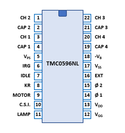
The TMC0595 uses a standard 0.4” wide 22-pin DIP (Dual In-line Package with a 0.1” / 2.54 mm lead pitch).
| Pin | IO | Function | Pin | IO | Function |
| 1 | A | R/W Track 2 | 22 | A | R/W Track 3 |
| 2 | A | Capacitor Track 2 | 21 | A | Capacitor Track 3 |
| 3 | A | R/W Track 1 | 20 | A | R/WTrack 4 |
| 4 | A | Capacitor Track 1 | 19 | A | Capacitor Track 4 |
| 5 | V | Common Voltage | 18 | V | Reference Voltage |
| 6 | O | Instruction words | 17 | V | Common Voltage |
| 7 | I | Calculating status | 16 | I | External access |
| 8 | O | Keyboard emulation | 15 | I | Clock Input 2 |
| 9 | O | Motor on/off | 14 | I | Clock Input 1 |
| 10 | I | Card Sensing Input | 13 | V | Negative Voltage VDD |
| 11 | O | Lamp | 12 | V | Negative Voltage VGG |
If you have additions to the above datasheet please email: joerg@datamath.org.
© Joerg Woerner, March 19, 2021. No reprints
without written permission.