DATAMATH CALCULATOR MUSEUM
|
DATAMATH CALCULATOR MUSEUM |
Cal-Tex Semiconductor, Inc. was founded in 1971 by former Texas Instruments and Nortec employees in Richardson, Texas, as a manufacturer of integrated circuits (ICs) for electronic calculators. The company later established operations in Santa Clara, California, with financial backing from Japan's Eiko Business Machine Co., Ltd., better known under its Unitrex brand.
When Mostek introduced in November 1970 with the MK6010 the World’s first "single-chip calculator circuit", it was sold exclusively to Nippon Calculating Machine Corp of Japan for their Busicom Model 120-DM small desktop calculator, also known as Busicom Junior, and not available to other customers. Recognizing the resulting gap in the market, Cal-Tex immediately began developing a fully functional, pin-compatible replacement. Formally introduced in November 1971 - exactly one year after the original MK6010 - and with first silicon available in January 1972, the CT5001 quickly found its first major design win in the highly successful Unitrex 1200 (Type 27) desktop calculator.
Busicom recognized the potential of Mostek's ion-implantation process, which led to the introduction of the low-voltage, low-power MK6010L in February 1971. The first application of the MK6010L was a remarkably compact, battery-operated handheld calculator with LED displays - quite the opposite of the original MK6010, which had been designed for a large, AC-powered desktop calculator with a VFD. Although Busicom succeeded in squeezing the required DC/DC converter and LED drivers into an exceptionally compact housing, the manufacturing costs of the LE-120A and its successor, the LE-120S, remained prohibitively high.
Early in 1972, Cal-Tex carefully analyzed the requirements for an alternative to the MK6010L. The result was the CT5002, introduced in August 1972 as a single-supply version of the CT5001 optimized for portable, battery-powered calculators with LED displays.
The CT5002 offered several advantages over the MK6010L, enabling more cost-effective calculator designs:
|
• Single-supply voltage of VDD =
−6 V • Integrated 2-phase clock generation from 1-phase clock input • Positive logic of Digit and Segment outputs for easy interfacing to LED Displays • Display inhibit feature for power conservation |
The first high-volume design win for the CT5002 was the Caltronic 812 calculator, with an estimated production volume of approximately 100,000 units.
When Busicom started early in 1972 to struggle financially and decided to forfeit its right of exclusivity, Mostek rebranded the MK6010 to MK5011 and its low power sibling MK6010L to MK5012. Cal-Tex followed with the CT5012, their low-power version of the CT5001. To date, we have not identified a single calculator design incorporating the CT5012, nor have we found any evidence that the device ever entered production.
Nevertheless, by late 1972 and early 1973, the CT5002, CT5012, the 12-digit MK5012, and the 10-digit MK5010 - all descendants of the MK6010 introduced in November 1970 - had become increasingly difficult to sell in the face of more highly integrated and versatile calculator chipsets offered by Texas Instruments, Rockwell, and other competitors. Cal-Tex responded shortly thereafter with the introduction of its CT5030 single-chip calculator circuit while Mostek added the MK5020 to their portfolio.
QUICK-LINK to Cal-Tex Calculator Integrated Circuits.
| Type | Calculators | Keyboard | Constant (M-D-A-S) |
Digits | Fixed DP | Rounding | Special Functions |
Seg./Dig. Blanking |
(6,7,9) Font |
Entry Overflow Calculating Overflow |
| CT5002 | Caltronic 812 | [+=][−=] | X-X-X-X | 12 | [0,2,3,4] | None | Display Inhibit |
S1, S8 NONE |
 |
 |
| Description | Comments | |
| Architecture | Single-chip Calculator | First Generation |
| Category | Register Processor | Bit-serial |
| Related | CT5001 LIT-019 |
Original design Litronix Branding |
| ROM Size | n.a. | |
| RAM Size | 108 Bits | 2 Registers * 48 Bits (12 Digits) 12 Status Bits |
| Outputs | 12 Digits 9 Segments 1 Status |
External LED Digit Drivers External LED Segment Drivers Sign |
| Inputs | 4 Keyboard 6 Keyboard 2 Decimal Select 1 Clear |
Numerals BCD Functions Discrete 0, 2, 3, 4 Active Low |
Capacity: Up to 12 digits (positive and negative)
Logic: Algebraic Adding Machine Logic
[2] [x] [3] [+=] [4] [x] [5] [+=] → '20.'
Number Entry: Right-justified number entry, entering a thirteenth digit is resulting in an overflow condition and is only recoverable using the [C] key
[0 2 3 4]: [1] [2] [3] [4] [5] [6] [7] [8] [9] [0] [1] [2] [3] → '00000000.0.0.0.0.'
Decimal Point: First entered decimal point is used, additional decimal point entries are ignored
[0 2 3 4]: [1] [.] [2] [.] [3] → '1.23'
Fixed Decimal Point: The decimal point can be set to [0 2 3 4] digits
[0 2 3 4]: [1] [+=] [2] [+=] → '3.000'
Clear: Automatic power-up clear implemented. [C] key clears the whole calculator, [CE] key clears last entry of a number
[0 2 3 4]: [1] [+=] [2] [C] [3] [+=] → '3.'; [1] [+=] [2] [CE] [3] [+=] → '4.'
Change Sign: Not supported. When performing multiplication or division, a negative value can only be assigned to the first number by pressing the [−=] key after entering the number
[0 2 3 4]: [2] [−=] [x] [3] [+=] → '-6.'; [2] [x] [3] [−=] → '-1.'
Number Display: Right-justified number display with leading-zero suppression
Negative Numbers: Negative numbers are shown with an active signal at a dedicated output pin and usually connected to a discrete LED indicator
Calculating Overflow: An overflow results in displaying all zeros with the five rightmost decimal points lit and is only recoverable using the [C] key
[0 2 3 4]: [1] [2] [3] [4] [5] [x] [1] [2] [3] [4] [5] [+=] → '00000000.0.0.0.0.', [C] → '0.0000'
Divide By Zero: A division of a positive or negative number by zero results in an infinity loop with the display blanked and is only recoverable using the [C] key
[0 2 3 4]: [1] [:] [0] [+=] → ' ', [C] → '0.'
Display Test: Pressing the [C] or [CE] key lit up all 12 digits of the display
[C] → '000000000000', [CE] → '000000000000'
Rounding: Rounding of displayed calculating results is not supported
[0 2 3 4]: [2] [0] [:] [3] [+=] → '6.666'
Known Calculator Logic Bugs:
Negative Zero Bug : Certain calculations result in displaying a negative zero
[0 2 3 4]: [1] [−=] → '-1.', [1] [+=] → '-0.'
Divide to Negative Zero Bug: Certain calculations result in displaying a negative zero
[0 2 3 4]: [0] [.] [0] [0] [0] [1] [−=] → '-0.0001', [:] [1] [0] [+=] → '-0.0000'
Fix Point Switch Bug: Changing the position of the Fix Point Switch during number entry leads to unexpected results
[0 2 3 4]: [1] [.] [2] [3] → '1.23', [0 2 3 4]: [+=] → '1230000'
Twelfth Digit Multiplication Bug: Multiplications with the sum of digits for multiplicand and multiplier larger than twelve result in an overflow
[0 2 3 4]: [1] [2] [3] [4] [5] [6] [7] [8] [9] [0] [1] [2] [x] → '123456789012.', [1] [+=] → '0.0.0.0.0.0.0.0.0.0.0.0.'
[0 2 3 4]: [6] [5] [4] [3] [2] [1] [x] → '654321.', [6] [5] [4] [3] [2] [1] [+=] → '428135971041.'
Twelfth Digit Division Bug: Divisions with the dividend or the divisor larger than eleven digits result in an overflow
[0 2 3 4]: [1] [2] [3] [4] [5] [6] [7] [8] [9] [0] [1] [2] [:] → '123456789012.', [1] [+=] → '0.0.0.0.0.0.0.0.0.0.0.0.'
[0 2 3 4]: [1] [:] → '1.', [1] [2] [3] [4] [5] [6] [7] [8] [9] [0] [1] [2] [+=] → '0.0.0.0.0.0.0.0.0.0.0.0.'
ABSOLUTE MAXIMUM RATINGS
| Item | Min | Typ | Max | Unit | Comments |
| VDD | -12.0 | 0.3 | V | to VSS | |
| VOUT | -12.0 | 0.3 | V | ||
| VIN | -12.0 | 0.3 | V |
RECOMMENDED OPERATING CONDITIONS
| Item | Min | Typ | Max | Unit | Comments |
| VSS | 0 | V | |||
| VDD | -7.5 | -6.0 | -5.5 | V | |
| VIH | VSS-1.5 | VSS | V | ||
| VIL | VDD | VDD+1.5 | V | ||
| Ext. CK | 20 | 40 | 50 | kHz | Two-phase clock |
ELECTRICAL CHARACTERISTICS
| Item | Min | Typ | Max | Unit | Comments |
| IDD | 5 | 10 | mA | VDD = -6.0 V | |
| IDD | 8 | 16 | mA | VDD = -7.5 V | |
| ION1 | -1.0 | mA | VOT = -0.5 V | ||
| ION2 | -5.0 | mA | VOT = -2.0 V | ||
| IOFF1 | -50 | uA | Clock Outputs, VOT = -7.5 V | ||
| IOFF2 | -25 | uA | All Other Outputs, VOT = -7.5 V | ||
| IIH | 1 | uA | CKIN, D.I., DP1, DP2, Positive Logic | ||
| IIH | -150 | uA | All Other Inputs, Negative Logic (internal resistors to VSS) |
DISPLAY TESTING
Pulling the KC or KCE Inputs of the CT5002 to VDD (log.1) by pressing the [C] or [CE] keys is resulting in all Segment Outputs SA to SH activated for the 12 Digit Outputs D1 to D12, displaying '000000000000'.
Pulling the KC or KCE Inputs of the CT5002 back to VSS (log.0) by releasing the [C] or [CE] clears the display.
CALCULATING OVERFLOW
An overflow condition of the CT5002 is resulting in the Segment Outputs SA to SF activated for the 12 Digit Outputs D1 to D12 and SDP activated for the 5 Digit Outputs D1 to D5, displaying '00000000.0.0.0.0.'.
The overflow condition is only recoverable using the [C] key.
DIVIDE BY ZERO LOOP
A division of a positive or negative number by zero of the CT5002 is resulting in the Segment Outputs SA to SF disabled, SG activated and SDP pulsing while the 12 Digit Outputs D1 to D12 are disabled, hence blanking the display.
The Divide by Zero Loop is only recoverable using the [C] key.
DISPLAY INHIBIT
Pulling the Display Inhibit (D.I.) Input of the CT5002 to VSS (log.1) is resulting in the Segment Outputs SB, SC, SE, SF and SG activated for Digit Output D1 and all Segment Outputs deactivated for all other Digit Outputs, displaying 'H' to signal the "Display Hold" status.
Pulling the Display Inhibit (D.I.) Input of the CT5002 back to VDD (log.0) restores the display.
DIGIT DRIVERS
The CT5002 single-chip calculator circuit is manufactured in a PMOS process and its Digit Outputs are high-side PMOS transistors. For easy interfacing to LED displays, an activated digit corresponds to a logical 1 or closed output. All other, non-activated digits have the PMOS transistors turned off. We characterized here at the Datamath Calculator Museum the Digit Driver Output pin D2 of an CT5002 and measured an output resistance of around 200 Ohm at an Output Voltage of -1.0 V.
SEGMENT DRIVERS
The CT5002 single-chip calculator circuit is manufactured in a PMOS process and its Segment Outputs are high-side PMOS transistors. For easy interfacing to LED displays, an activated segment corresponds to a logical 1 or closed output. We characterized here at the Datamath Calculator Museum the Segment Driver Output pin SG of an CT5002 and measured an output resistance of 200 Ohm at an Output Voltage of -1.7 V.
The Datamath Calculator Museum DCM-50A (PLAYGROUND) supports the Characterization of the CT5002 single-chip calculator circuit using the DCM-50A Playground MK6010 Adapter with multiple tweaks:
| • DCM-50A PG MK6010 Family Adapter mounted on top of the
DCM-50A PG Frame Carrier (Non-inverting Digit and Segment Outputs) • Selector Jumper for set to low-voltage (6...15 V) Chips (6 V Supply) • CK1 and CK2 Jumpers at CT5002 removed and CT5002 Pins connected to DIN21 and DIN22 Pins (CK1 and CK2 Out Load Resistors) • VGG Jumper at CT5002 removed and CT5002 Pin connected to CK1 Pin (Clock Input) • SH Jumper at CT5002 removed and CT5002 Pin connected to VDD (Display Enable Input) • SIGN Jumper at CT5002 and SIGN POL Jumper removed and CT5002 Pin connected to right Pin of SIGN POL Jumper (Sign Polarity) |
The optional DCM-50A Playground Digilent I/O Extender supports
Characterization
and
Reverse-engineering of CT5001 single-chip calculator circuits.
The CT5002 is using a standard 0.6” wide 40-pin CDIP (Ceramic Dual In-line Package with a 0.1” / 2.54 mm lead pitch) or 0.6” wide 40-pin DIP (Dual In-line Package with a 0.1” / 2.54 mm lead pitch).
The die of the CT5002 is attached to the lead frame of the 40-pin DIP with its Pin 1 (VSS) directly connected to the paddle and silicon die.
The CT5002 was manufactured in a 10 um metal gate PMOS process (metal width = 0.40 mil / 10.0 um, metal spacing = 0.40 mil / 10.0 um, diffusion width = 0.40 mil / 10.0 um, diffusion spacing = 0.40 mil / 10.0 um).
The die size of the CT5002 is approximately 185 mils * 170 mils / 4.7 mm * 4.3 mm.
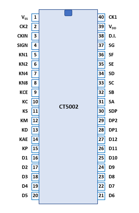
| Pin | IO | Function | Pin | IO | Function |
| 1 | V | Common Voltage VSS | 40 | O | Clock Phase 1 |
| 2 | O | Clock Phase 2 | 39 | V | Negative Voltage VDD |
| 3 | I | Clock Input | 38 | I | Display Inhibit |
| 4 | O | Sign driver | 37 | O | Segment driver G |
| 5 | I | Encoded Key input '1' | 36 | O | Segment driver F |
| 6 | I | Encoded Key input '2' | 35 | O | Segment driver E |
| 7 | I | Encoded Key input '4' | 34 | O | Segment driver D |
| 8 | I | Encoded Key input '8' | 33 | O | Segment driver C |
| 9 | I | Key input [CE] | 32 | O | Segment driver B |
| 10 | I | Key input [C] | 31 | O | Segment driver A |
| 11 | I | Key input [−=] | 30 | O | Segment driver DP |
| 12 | I | Key input [x] | 29 | I | Decimal Point Sel.2 |
| 13 | I | Key input [:] | 28 | I | Decimal Point Sel.1 |
| 14 | I | Key input [+=] | 27 | O | Digit driver 12 (MSD) |
| 15 | I | Key input [.] | 26 | O | Digit driver 11 |
| 16 | O | Digit driver 1 (LSD) | 25 | O | Digit driver 10 |
| 17 | O | Digit driver 2 | 24 | O | Digit driver 9 |
| 18 | O | Digit driver 3 | 23 | O | Digit driver 8 |
| 19 | O | Digit driver 4 | 22 | O | Digit driver 7 |
| 20 | O | Digit driver 5 | 21 | O | Digit driver 6 |
| The Segment drivers A-G and DP (Decimal Point) are connected to the display in the pictured way. | 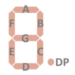 |
The keyboards of all calculators based on the CT5002 consist of 10 number keys connected between VDD or VGG (log.1) with a diode matrix to the key inputs KN1 to KN4 (Numbers) and 7 function keys connected between VDD or VGG (log.1) to discrete key inputs. The position of the Decimal Point is selected with 2 additional switch inputs DP1 and DP2.
CT5002 | ||||
| KEY | KN8 | KN4 | KN2 | KN1 |
| [1] | - | - | - | log.1 |
| [2] | - | - | log.1 | - |
| [3] | - | - | log.1 | log.1 |
| [4] | - | log.1 | - | - |
| [5] | - | log.1 | - | log.1 |
| [6] | - | log.1 | log.1 | - |
| [7] | - | log.1 | log.1 | log.1 |
| [8] | log.1 | - | - | - |
| [9] | log.1 | - | - | log.1 |
| [0] | log.1 | - | log.1 | - |
CT5002 | |||||||
| KEY | KC | KCE | KD | KM | KS | KAE | KP |
| [C] | log.1 | - | - | - | - | - | - |
| [CE] | - | log.1 | - | - | - | - | - |
| [÷] | - | - | log.1 | - | - | - | - |
| [×] | - | - | - | log.1 | - | - | - |
| [−=] | - | - | - | - | log.1 | - | - |
| [+=] | - | - | - | - | - | log.1 | - |
| [.] | - | - | - | - | - | - | log.1 |
CT5002 | ||
| SWITCH | DP2 | DP1 |
| [4-3-2-0] | - | - |
| [4-3-2-0] | - | log.1 |
| [4-3-2-0] | log.1 | - |
| [4-3-2-0] | log.1 | log.1 |
Scanning is performed in D1 → D12 direction at a rate of about 380 Hz:
|
• State Time = 1 Clock =
0.025 ms @ CK=40 kHz • Digit Time = 8 States = 0.200 ms @ CK=40 kHz • Scan Time = 13 Digit Times (D1 to D13 with D13 a dead cycle) = 2.6 ms @ CK=40 kHz |
Calculators based on the CT5002 typically make use of of 8-digit LED (Light-Emitting-Diode) Displays with common cathode architecture.

If you have additions to the above datasheet please email: joerg@datamath.org.
© Joerg Woerner, July 1, 2026. No reprints
without written permission.