DATAMATH CALCULATOR MUSEUM
|
DATAMATH CALCULATOR MUSEUM |
Texas Instruments introduced on May 24, 1977 the now legendary TI Programmable 59 and its sibling TI-58, featuring a novelty, the Solid State Software Modules™ with up to 5,000 program steps. A small lid on the backside of the TI-58/TI-59 allowed for easy access to the modules roughly the size of thumb tip.
The Master Library, known as "Module -1-", with 25 different programs was included with the TI-58 and TI-59. Twelve additional Solid State Software Modules™, known as "Module -2- to -13-" were available from Texas Instruments as Standard Libraries. Due to this innovative module concept both the TI-58 and TI-59 gained a lot of attention and dozens of Modules were released for applications ranging from Insurance Fee Calculations to Tax Calculations to Screw Joint Calculations, HVAC Design, Pool Water Analysis and even Flight Computers for the USMC Harrier.
Each of these Modules contains a Mask-ROM (Read-Only Memory programmed during the manufacturing process) in a small 8-pin package connected serially to the TMS0500 Building Blocks for Scientific and Programmable Calculators used with the TI-58/TI-59 and introduced already in 1974 with the SR-50 calculator. While the 13-Bit instructions for the TMC0501 Arithmetic Chip are stored in SCOM (Scanning and 1k*13 Bits Read-Only Memory), DSCOM (SCOM with 2.5k*13 Bits ROM), or BROM (Bare ROM with 1k*13 Bits, no scanning) Chips, are user programs stored as Opcodes or "merged keystrokes" encoded in two BCD (Binary Coded Decimal) digits for a combined 8-bit data size. Storing user data is accomplished by concatenating eight program steps into one data register. Keystroke programmable calculators based on the TMS0500 Architecture like the SR-52 and SR-56 store user programs and user data in PRAM (Program Random-Access Memory) Chips with a capacity of 1,920 Bits or 240 program steps/30 data registers accessed through a 4-bit I/O bus. Calculators with an integrated reader for magnetic cards allow loading and archiving of user programs and user data accordingly.
While the pin-out of the TMC0540 CROM (Customer Read-Only Memory) is identical with the TMC0560 BROM (Bare Read-Only Memory), are their architectures completely different:
|
• TMC0540: 5,000*8 Bits capacity, 4-digit BCD address (0000-4999), two BCD digits Opcodes • TMC0560: 1,024*13 Bits capacity, 10-bit Binary address (0x000-0x3FF), 13-bit Instruction Words |
Accessing the TMC0540
CROM is established with four different commands:
|
• LOAD PC: Sets memory address pointer to 4-digits BCD value, LSD first with 0000 to 9994 • FETCH: Reads two BCD digits and increments address by 1, lower nibble first • FETCH HIGH: Reads upper BCD digit and does not increment address • UNLOAD PC: Reads current memory address pointer as 4-digits BCD value, LSD first |
The Master Library or "Module -1-" provided with the TI-58/TI-58C/TI-59 calculators uses a TMC0540
Chip with the marking TMC0541,
"Module -2-" is marked TMC0542 and so on. Modules manufactured for third parties are marked with TMC0540 and a ROM-Code identification
"ZA55xx" and later adopted to the TI-Standard for Consumer Group Products with a leading
"CD56xx" or "CD57XX".
QUICK-LINK to TMS0500 Family.
| CROM | Top Markings Bottom Markings |
Module Markings Additional Module Markings |
Second ROM ©Texas Instruments |
Key Code Programs ©Texas Instruments |
| TMC0541 | TMC0541NL ASP7749 |
MASTER LIBRARY MODULE -1- TI ©1977 1014976-1 |
||
| TMC0542 | TMC0542NL BSP7901 |
APPLIED STATISTICS MODULE -2- TI ©1977 1014976-2 |
||
| TMC0543 | TMC0543NL SP7731 |
R.E./INVESTMENT MODULE -3- TI ©1977 1014976-3 |
||
| TMC0544 | TMC0544NL ASP7849 |
SURVEYING MODULE -4- TI ©1977 1014976-4 |
||
| TMC0545 | TMC0545NL SP7727 |
MARINE NAVIGATION -5- TI ©1977 1014976-5 |
||
| TMC0546 | TMC0546NL SA7723 |
AVIATION MODULE -6- TI ©1977 1014976-6 |
||
| TMC0547 | TMC0547NL SP7740 |
LEISURE LIBRARY MODULE -7- TI ©1977 1014976-7 |
||
| TMC0548 | TMC0548NL BSA7812 |
SECURITIES ANALYSIS MODULE -8- TI ©1978 1014976-8 |
||
| TMC0549 | TMC0549NL ASA7832 |
BUSINESS DECISIONS MODULE -9- TI ©1978 1014976-9 |
||
| TMC0550 | TMC0550NL SP7927 |
MATH/UTILITIES MODULE -10- TI ©1978 1014976-10 |
||
| TMC0551 | TMC0551NL SP7936 |
EE LIBRARY MODULE -11- TI ©1978 1015017-101 |
||
| TMC0553 | TMC0553NL ASP8040 |
STRUCTURAL ENGINEERING MODULE REV.A TI ©1981 |
||
| TMC0554 | TMC0554NL SP7914 |
AGRICULTURE MODULE -12- ISU ©1981 TI ©1979 |
||
| TMC0555 | TMC0555NL ASP8009 |
RPN SIMULATOR MODULE -13- TI ©1978 1014976-103 |
||
| TMC0540 ZA5507 |
ZA5507NL DBS323 |
SCHENCK BALANCING MODULE CAB 1978 | ||
| TMC0540 ZA5511 |
TMC0540NL ZA5511 SP8106 |
IMCO DRIL MOD | ||
| TMC0540 ZA5535 |
TMC0540NL ZA5535 SP7936 |
ALLIANZ LEBEN -1- | ||
| TMC0540 ZA5537 |
TMC0540NL ZA5537 SP7936 |
SCHENK NAVIPROG 2000 | ||
| TMC0540 ZA5538 |
TMC0540NL ZA5538 SP7932 |
BMF VERMESSUNG (BAYERN)0540/ZA5538 | ||
| TMC0540 ZA5560 |
TMC0540NL ZA5560 |
SPECIAL SITUATION 11784975 REV- |
||
| TMC0540 ZA5568 |
TMC0540NL ZA5568 DBS249 |
155MM M109A1 11784967 REV- |
||
| TMC0540 ZA5574 |
TMC0540NL ZA5574 |
SURV CROM II |
||
| TMC0540 ZA5613 |
TMC0540NL ZA5613 |
CEMENTING MODULE -1- Halliburton 1980 |
||
| TMC0540 ZA5665 |
TMC0540NL ZA5665 |
COPRHEAD 155MM 11785344 PROV |
||
| TMC0540 CD5713 |
CD5713NL QBS 8527 PHILIPPINES |
ALLIANZ 2 |
IMPORTANT NOTE: This information is provided as a service of the Datamath Calculator Museum to enthusiasts of early Texas Instruments calculators and please be aware that the Copyright of the Software transcribed in the ROM Images, the underlying algorithm or application might be owned by Texas Instruments or other third parties. The commercial use of the published Recorded ROM Images is strictly prohibited. In case of questions please contact us using the email address listed in the footer of this webpage.
Note: A comprehensive list of all known TMC0540 CROMs can be found here.
| Item | Min | Typ | Max | Unit | Comments |
| VSS | 0 | V | |||
| VDD | -10.5 | -10.0 | -9.5 | V | |
| VGG | -16.3 | -15.8 | -15.3 | V | |
| PHI1, PHI2 | 225 | 230 | kHz | Opposite phases |
CROM MEMORY
The TMC0540 CROM (Customer Read-Only Memory) integrates 5,000*8 Bits Key Code Memory with serial interface to the TMC0501E Arithmetic Chip to easily access a library of programs with the TI-59, TI-58C and TI-59 Series of Programmable Calculators. The TMC0540 Chips are using a 4-digit BCD (Binary Coded Decimal) Address and 2-digit BCD Data stored in 8-bit words. While the Pin Configuration of the TMC0540 is identical with the TMC0560 BROM (Bare Read-Only Memory) Chip, use the two devices a completely different method to load a memory address and retrieve its data. Texas instruments accordingly describes the TMC0540 in some of its patent applications as "Second ROM" while the TMC0560 is labeled - as the TMC0520, TMC0530 and TMC0580 - "First ROM" or Instruction Memory. To access Instructions from its ROM Chips, the TMC0501E Arithmetic Chip transmits the 13-bit ROM Address serially through its EXT Output and receives the 13-bit Instruction Words serially through its IG Input using the 16 State Times S0 to S15 of is Instruction Cycle:
|
• S0: PREG - Program
Register Signal to load the address counter with a 10-bit ROM Address • S1: COND - Condition Signal to allow for conditional branches • S2: HOLD - Hold Condition Signal to suppress auto-increment or decrement of the address counter • S3 - S12: lower 10-bit ROM Address (LSB first) • S13 - S15: upper 3-bit ROM Address (MSB last) for CS0 - CS7 |
The interface between the TMC0501E Arithmetic Chip and the TMC0540 "Second ROM" uses the same EXT and IRG pins but changes the signal directions. The TMC0540 "listens" on its IRG Input and decodes one of four instructions that the "First ROM" is transmitting to the TMC0501E. Bases on these instruction, the TMC0540 either "listens" on its bidirectional EXT pin or "talks" on it, a method called half-duplex communication to annotate that transmission is possible in both ways but not at the same time as with full-duplex communication:
|
• LOAD PC: Sets memory address pointer to 4-digits BCD value, LSD first with 0000 to 9994 • FETCH: Reads two BCD digits and increments address by 1, lower nibble first • FETCH HIGH: Reads upper BCD digit and does not increment address • UNLOAD PC: Reads current memory address pointer as 4-digits BCD value, LSD first |
The TMC0540 CROM is divided into two partitions, the first part of the memory is used for housekeeping purposes and the second, larger part of the 5,000*8 Bits is used to store the actual Key Codes of the Programs contained in the Solid State Software Modules (SSSM). The housekeeping portion is realized in a pretty straightforward manner and contains the number of programs stored in the SSSM, an optional Copy Protection Flag for the programs, pointers to the starting addresses of the individual programs and a pointer indicating the position of the last Key Code address used only for program size calculation of the last program stored in the SSSM:
| Address 4-digit BCD |
Size 2-digit BCD |
Description |
| 0000 | 1 | Number of Programs (N), 01-99 |
| 0001 | 1 | Copy Protection Flag (C), 00: Not protected, 01: Protected |
| 0002 | 2 | 4-digit BCD Address Program 1 (PRG1) |
| 0004 | 2 | 4-digit BCD Address Program 2 (PRG2) |
| - - | 2 | - - |
| 00[2N] | 2 | 4-digit BCD Address Program N (PRGN) |
| 00[2N]+2 | 2 | 4-digit BCD Pointer to last Key Code of Program N + 1 (PRGS) |
| PRG1 | 1 | First 2-digit BCD Key Code of Program 1 |
| PRG1+1 | 1 | Second 2-digit BCD Key Code of Program 1 |
| - - | 1 | - - |
| PRG2-1 | 1 | Last 2-digit BCD Key Code of Program 1 |
| PRG2 | 1 | First 2-digit BCD Key Code of Program 2 |
| - - | 1 | - - |
| PRGN-1 | 1 | Last 2-digit BCD Key Code of Program N-1 |
| PRGN | 1 | First 2-digit BCD Key Code of Program N |
| - - | 1 | - - |
| PRGS-1 | 1 | Last 2-digit BCD Key Code of Program N |
| PRGS | 1 | First 2-digit BCD Key Code "92" (INV SBR) of Empty CROM Space |
| - - | 1 | - - |
| 4999 | 1 | Last 2-digit BCD Key Code "92" (INV SBR) of Empty CROM Space |
Retrieving the physical memory content a TMC0540 CROM is possible in different ways, keep in mind that loading the programs into the calculator memory would only copy the Key Codes of the program if it is not copy protected and not to large:
|
• Removing the silicon chip from the plastic encapsulation and visually read the individual bits of the memory and map them to the memory address and data position • Observing the communication on the IRG and EXT signals between TMC0501E Arithmetic Chip and TMC0540 CROM while the calculator is accessing the SSSM • Reading the content of the TMC0540 CROM with additional hardware to emulate the TMC0501E Arithmetic Chip |
Read more about the Birth of the DCM-0500 Platform developed to study the TMC0540 CROM Chips and gradually extended to Reverse-engineer all ROM Chips introduced with the TMS0500 Building Blocks.
 Electronically recording the physical memory content of the TMC0541
CROM
used with Texas Instruments' Master Library included with the TI-58, TI-58C
and TI-59 Series of Programmable Calculators and analyzing as example
Program ML-24 Unit Conversions (1) further explains the organization of the
stored data.
Electronically recording the physical memory content of the TMC0541
CROM
used with Texas Instruments' Master Library included with the TI-58, TI-58C
and TI-59 Series of Programmable Calculators and analyzing as example
Program ML-24 Unit Conversions (1) further explains the organization of the
stored data.
The first 4-digit BCD address "0000" shows with "25" the number of programs stored in the SSSM, the value "0" in BCD address "0001" allow copying the program into the calculator memory and BCD addresses "0002" and "0003" point to the begin of Program 1 at "0054". BCD addresses "0048" and "0049" point to address "4672", the starting point of Program 24. Here at address "4672" and following, we easily recognize the Key Codes of the "inches to centimeters" conversion performed with the [A] key, a simple multiplication of the value in the display by 2.54: "76" "11" "53" "24" "65" "02" "93" "05" "04" "54" "92" or [2nd] [LBL] [A] [(] [CE] [*] [2] [.] [5] [4] [)] [INV] [SBR].
TI-58/58C/59 KEY CODES
The TI-58, TI-58C and TI-59 Programmable Calculators can store a sequence of instructions in their TMC0598 Multi-Register Chips (TI-58, TI-59) or Static Random Access Memory Chip (TI-58C) and execute them accordingly. The calculators provide four different ways to enter the instructions into the volatile (TI-58, TI-59) or non-volatile (TI-58C) Memory Chips:
|
• [LRN]: The instructions are
entered manually with keystrokes of the calculator keyboard into the Memory Chips • [SSSM]: The instructions are copied from the Solid State Software Module into the Memory Chips • [CONST]: The instructions are copied from the Constant and Key Code DSCOM into the Memory Chips • [MAG IO]: The instructions are loaded from the magnetic card reader (TI-59 only) into the Memory Chips |
The TI-58, TI-58C and TI-59 Series of Programmable Calculators uses the Decimal Numbers "00" to "99" for its Opcodes or Key Codes, most instructions are coded directly with their corresponding X/Y-position on the keyboard matrix with the keys [0]-[9] directly mapped into Key Codes 00 to 09 and the freed-up numbers used for merged keystrokes:
| Keycode (BCD) |
_0 | _1 | _2 | _3 | _4 | _5 | _6 | _7 | _8 | _9 |
| 0_ | [0] | [1] | [2] | [3] | [4] | [5] | [6] | [7] | [8] | [9] |
| 1_ | [2nd][E] | [A] | [B] | [C] | [D] | [E] | [2nd][A] | [2nd][B] | [2nd][C] | [2nd][D] |
| 2_ | [2nd][CLR] | [2nd] | [INV] | [lnx] | [CE] | [CLR] | [2nd][2nd] | [2nd][INV] | [2nd][log] | [2nd][CP] |
| 3_ | [2nd][tan] | [LRN] | [x<>t] | [x2] | [√x] | [1/x] | [2nd][Pgm] | [2nd][P→R] | [2nd][sin] | [2nd][cos] |
| 4_ | [2nd][Ind] | [SST] | [STO] | [RCL] | [SUM] | [yX] | [2nd][Ins] | [2nd][CMs] | [2nd][Exc] | [2nd][Prd] |
| 5_ | [2nd][|x|] | [BST] | [EE] | [(] | [)] | [÷] | [2nd][Del] | [2nd][Eng] | [2nd][Fix] | [2nd][Int] |
| 6_ | [2nd][Deg] | [GTO] | [2nd][Pgm] [2nd][Ind] |
[2nd][Exc] [2nd][Ind] |
[2nd][Prd] [2nd][Ind] |
[×] | [2nd][Pause] | [2nd][x=t] | [2nd][Nop] | [2nd][Op] (Note) |
| 7_ | [2nd][Rad] | [SBR] | [STO] [2nd][Ind] |
[RCL] [2nd][Ind] |
[SUM] [2nd][Ind] |
[−] | [2nd][Lbl] | [2nd][x≥t] | [2nd][∑+] | [2nd][x] |
| 8_ | [2nd][Grad] | [RST] | (Note) | [GTO] [2nd][Ind] |
[2nd][Op] [2nd][Ind] |
[+] | [2nd][St flg] | [2nd][If flg] | [2nd][D.MS] | [2nd][PI] |
| 9_ | [2nd][List] | [R/S] | [INV][SBR] | [.] | [+/−] | [=] | [2nd][Write] | [2nd][Dsz] | [2nd][Adv] | [2nd][Prt] |
Notes: Key Code "82" is used for Hierarchy Address and is not accessible with keystrokes and has like Key Code "69" [2nd] [Op] additional parameters.
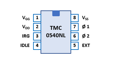
The TMC0540 was manufactured in a 6 um metal gate PMOS process (metal width = 0.25 mil / 6.0 um, metal spacing = 0.25 mil / 6.0 um, diffusion width = 0.20 mil / 5.0 um, diffusion spacing = 0.30 mil / 8.0 um).
The TMC0540 uses a standard 0.3” wide 8-pin DIP (Dual In-line Package with a 0.1” / 2.54 mm lead pitch).
| Pin | IO | Function | Pin | IO | Function |
| 1 | V | Negative Voltage VGG | 8 | V | Common Voltage |
| 2 | V | Negative Voltage VDD | 7 | I | Clock Input 1 |
| 3 | I | Instruction words | 6 | I | Clock Input 2 |
| 4 | I | Calculating status | 5 | IO | External access |
If you have additions to the above datasheet please email: joerg@datamath.org.
© Joerg Woerner, February 02, 2001. No reprints
without written permission.