DATAMATH CALCULATOR MUSEUM
|
DATAMATH CALCULATOR MUSEUM |
With the introduction of the SR-51-II in 1976 the original 28-pin DIP (Dual Inline Package) encapsulation used for the TMC0501 Arithmetic Chip was changed to a 28-pin SDIP (Shrink Dual Inline Package) roughly the size of a standard 20-pin DIP encapsulation and the TMC0580 DSCOM (Double Scanning and Read-Only Memory) Chip more than doubled the capacity of the larger TMC0520/TMC0530 SCOM Chips from 1k*13 Bits to 2.5k*13 Bits in a 28-pin SDIP housing paving the way for the TI Programmable 59.
The TMC0580 DSCOM Chip integrates 2.5k*13 Bits Instruction Memory with serial interface to the TMC0501E Enhanced Arithmetic Chip, 32 Constants mainly used for the calculation of transcendental functions with 16 digits, each accessible through a 4-bit bidirectional I/O bus and outputs for up to 16-digit display and keyboard scanning. In addition to the 5 Registers of the TMC0501E Enhanced Arithmetic Chip labeled A, B, C, D, and E integrates the SCOM Chip two additional Registers with 16 digits capacity each, and named accordingly Register F and Register G. The DSCOM Chip not only doubled the number of additional Registers but increased them from two to eight. A previously undocumented improvement of the TMC0580 DSCOM Chip carried over from the TMC0530 is an additional integrated two-phase clock generator that can be used as a bond-out option in a 30-pin DIP (Dual Inline Package) encapsulation or in a standard 28-pin DIP housing as used with the SR-51-II.
While the design of the TMC0580 DSCOM Chip would allow the use of multiple devices in one product, were most designs implemented with two TMC0580 and additional TMC0560 BROM Chips to increase program memory to the maximum addressable capacity of 8k*13 Bits. Only the SR-60A Prompting Desktop Calculator makes use of three DSCOM Chips.
Communication between the TMC0501E Enhanced Arithmetic Chip and the other family members of the TMS0500 Building Blocks for Scientific and Programmable Calculators is realized with multiple means:
|
• IDLE, PHI 1 and PHI 2
Signals are used to synchronize all peripherals connected to the TMC0501E
Enhanced Arithmetic Chip with the 16 States of its Instruction Cycle • EXT Output indicates that the TMC0501E Enhanced Arithmetic Chip is addressing external memories/registers • IRG Input to receive the 13-bit Instruction Words from the ROM of the TMC0580 • 4-bit bidirectional I/O Bus I/O 8, I/O 4, I/O 2, and I/O 1 to communicate with registers |
QUICK-LINK to TMS0500 Family.
| Type | Calculators | Function |
| TMC0581 | SR-51-II | DSCOM |
| TMC0582 | TI-58, TI-59 | DSCOM 1, with TMC0571 |
| TMC0583 | TI-58, TI-59 | DSCOM 2, with TMC0571 |
| TMC0584 | SR-60A | DSCOM 1 |
| TMC0585 | SR-60A | DSCOM 2 |
| TMC0586 | SR-60A | DSCOM 3 |
| TMC0587 | TI-5230 | DSCOM 1, with TMC0572 |
| TMC0588 | TI-5230 | DSCOM 2, with TMC0572 |
| TMC0580/CD2400 | TI-58C | DSCOM 1, with TMC0573 |
| TMC0580/CD2401 | TI-58C | DSCOM 2, with TMC0573 |
| Revision | Products | First Prototypes | Comments |
| TMC0581 | SR-51-C (SR-51-II) | Initial design | |
| TMC0581 Rev A | SR-51-C (SR-51-II) | May 1976 | 6 [:] 0 [=] [SUM] → [INV] [SUM] |
| TMC0581 Rev B | SR-51-C (SR-51-II) | August 1976 | |
| TMC0582 | SR-52 II (TI-59) | December 1976 | Initial design, DSCOM 1 |
| TMC0582 Rev A TMC0523 Rev A |
SR-52 II (TI-59) | January 1977 | Card protecting, etc. |
| TMC0582 Rev B TMC0523 Rev A |
SR-52 II (TI-59) | March 1977 | |
| TMC0583 | SR-52 II (TI-59) | December 1976 | Initial design, DSCOM 2 |
| TMC0583 Rev A TMC0523 Rev A |
SR-52 II (TI-59) | January 1977 | Card protecting, etc. |
| TMC0583 Rev B TMC0523 Rev A |
SR-52 II (TI-59) | March 1977 | |
| TMC0584 | SR-60A | May 1977 | Initial design, DSCOM 1 |
| TMC0584 Rev A TMC0523 Rev A |
SR-60A | July 1977 | Card protecting, etc. |
| TMC0585 | SR-60A | May 1977 | Initial design, DSCOM 2 |
| TMC0586 | SR-60A | May 1977 | Initial design, DSCOM 3 |
| DSCOM | Top Markings Bottom Markings |
Calculator Date Code |
Instruction ROM ©Texas Instruments |
Constant ROM ©Texas Instruments |
Key Code Program ©Texas Instruments |
| TMC0581 Rev B | TMC0581NL DSP7731 DP0581DS SINGAPORE |
SR-51-II LTA3677 |
|||
| TMC0582 | TMC0582NL IB7910 |
TI-59 ATA1979 |
|||
| TMC0583 | TMC0583NL DBS7910 SINGAPORE | TI-59 ATA1979 |
|||
|
TMC0580 CD2400 |
TMC0580NL CD2400 CS8022 SINGAPORE | TI-58C ATA2980 |
|||
| TMC0580 CD2401 |
TMC0580NL CD2401 CS8018K SINGAPORE | TI-58C ATA2980 |
| Item | Min | Typ | Max | Unit | Comments |
| VSS | 0 | V | |||
| VDD | -10.5 | -10.0 | -9.5 | V | |
| VGG | -16.3 | -15.8 | -15.3 | V | |
| PHI1, PHI2 | 225 | 230 | kHz | Opposite phases |
CLOCK GENERATOR
The TMC0580 DSCOM integrates like the TMC0530 SCOM a two-phase clock generator. The TMS0500 Building Blocks use two non-overlapping clock signals with 180° phase difference and a voltage swing between VSS and VGG. While the original SR-50 design introduced in January 1974 featured a discrete circuitry for the clock generation consisting of a free-running multivibrator using two transistors and an additional four transistors to define both shape and voltage levels of the two clock signals, used the SR-50A introduced in March 1975 an integrated oscillator SN97227 and a TP4011 Clock Buffer Chip (actually a CD4011A Quad 2 Input NAND Gate specified for a supply voltage of 15.8 Volts) manufactured in CMOS technology to condition the signals to the proper levels of the TMS0500 Building Blocks. As of today the SR-51-II is the only known application of the integrated clock generator of the TMC0580, both the TI-58 and TI-59 make use of a TP0240 clock generator or one of its many siblings TP0300, TP0301, TP0301A, TP0335.
The TMC0580 uses for the clock oscillator an additional bond pad on its die located between the VSS and D0 pins. Three different configurations are possible with the additional bond pad, depending on the target application:
|
• DIP-28 Encapsulation with
CLK signal bonded to Pin 14: Integrated clock oscillator, only known use
for in SR-51-II design • DIP-28 Encapsulation with D0 signal bonded to Pin 14: Integrated clock oscillator disabled, typical use like TI-58, TI-58C and TI-59 designs to maintain PC-100 Printer Cradle compatibility • DIP-30 Encapsulation with CLK signal bonded to Pin 14 and D0 bonded to Pin 15: No design discovered |
The integrated clock oscillator of the TMC0580 can be operated with three different circuitries to achieve the desired frequency stability:
|
• External resistor: Connecting
a resistor between the CLK pin and VGG
uses a small, internal capacitor of the TMC0580 to define the
frequency of the clock signal. A resistor value of 120 kOhm as used with the SR-51-II results in a clock frequency around 120 - 150 kHz • External resistor and external capacitor: Connecting a resistor between the CLK pin and VGG and a capacitor to VSS results in an improved stability of the clock frequency. Values 5.49 kOhm and 100 pF as located in the TI-5230 results in a clock frequency around 165 - 180 kHz • External resonator: Connecting a mechanical resonator made of high-stability piezoelectric lead zirconate titanate (PZT) between the CLK pin and VSS results in a very stability of the clock frequency allowing to write magnetic cards with one calculator and to read them with another one. |
KEYBOARD AND DISPLAY SCANNING
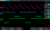
The TMS0500 Building Blocks use two non-overlapping clock signals PHI 1 and PHI 2 with a frequency of up to 250 kHz. Each so-called State Time consists of a sequence of PHI 1 → Pause 1 → PHI 2 → Pause 2 and represent the time for one bit to be operated on in the various sections of the chips. Sixteen of these State Times, numbered S0 to S15 represent one Digit Time used to scan the keyboard and display of the calculator. While the State Times count up from S0 → S1 ... → S15, are the Digit Times counting down from D15 → D14... → D0 to allow easier zero suppression approach of the displayed numbers. The TMC0501E Enhanced Arithmetic Chip generates an IDLE signal to synchronize the other TMC05xx chips to this timing sequence by marking the State Time S0 with its negative edge. The positive edge of the IDLE signal can occur anywhere between State Times S1 and S15, this feature is used to differentiate between the TMC0501E status "calculating" and "idle - display". Some calculator designs make use of the IDLE signal to lower the clock frequency in "display mode" to reduce power consumption of the chips
The TMS0500 Building Blocks share both the tasks of scanning the keyboard and display with the SCOM/DSCOM Chips responsible to generate and output the 16 Digit Times Output in descending order on its D0 to D15 pins, while the Arithmetic Chip or Enhanced Arithmetic Chip reads the input of the keyboard matrix on its 7 KN to KT pins and outputs the decoded signals for the display on its 9 Segment Output pins SA to SH and DP.
INSTRUCTION MEMORY
The TMC0580 DSCOM integrates a main Read-Only Memory (ROM) with 2,560*13 Bits as Instruction Memory for the TMC0501E Enhanced Arithmetic Chip. Internal, mask-programmed Chip-Select logic allow the use of a mix of up to one to three DSCOM and five to none TMC0560 BROM Chips in the design, limited to a maximum of 8,192 Words Memory Space. With the Arithmetic Chip fetching the first instruction after power-on from Address 0, feature all known calculator designs based on the TMC0580 at least one DSCOM addressed with the CS0 signal and hence covering an address range from 0x000 to 0x9FF (Decimal 0 to 2559). The innovative architecture of the TMS0500 Building Blocks allows not only the traditional loading of a ROM Address, additional logic inside the ROM addressing circuitry listens into the current instruction and based on additional signal even calculates the next ROM address. For this purpose the TMC0501E uses all 16 State Times S0 to S15 to communicate with its EXT Signal to the ROM Chips of the calculator:
|
• S0: PREG - Program
Register Signal to load the address counter with a 10-bit ROM Address • S1: COND - Condition Signal to allow for conditional branches • S2: HOLD - Hold Condition Signal to suppress auto-increment or decrement of the address counter • S3 - S12: lower 10-bit ROM Address (LSB first) • S13 - S15: upper 3-bit ROM Address (MSB last) for CS0 - CS7 |
The power-on circuitry of TMC0501E Enhanced Arithmetic Chip transmits on the EXT Signal for a few Digit Times a logical 1 at S0 time and logical 0 thereafter, effectively loading the address counter of the DSCOM with 0x000 and selecting the ROM responding to CS0.
CONSTANT AND KEY CODE MEMORY
A novel feature of the TMS0500 Building Blocks is a dedicated space for constants, frequently used with computing algorithm of trigonometric functions like sine, cosine, or tangent and number conversions like millimeters to inches. With typical serial architectures used in electronic calculators, one instruction would load just one digit of a number and consequently for numbers represented in Scientific calculators with 12 to 15 digits, the algorithm would tend to be rather slow. Texas Instruments introduced with the TMS0500 Building Blocks a novel approach to load constants containing 16 digits within one Digit Time or instruction cycle from the Constant Memory to the TMC0501E Enhanced Arithmetic Chip. To overcome the limitations of a bit-serial data transfer, the TMS0500 Architecture includes a 4-bit bidirectional I/O Bus I/O 8, I/O 4, I/O 2, and I/O 1. One digit, each of the 16-digit constants is transmitted during access to the Constant Memory in one State Time. Addressing of one of the possible 128 16-digit constants is accomplished with the EXT Signal connected to the SCOM Chips and a Constant Select logic "listening" into the "Recall Constant" instruction on IRG and outputting the constants accordingly on the I/O Bus.
|
• S0: Always log.0 to Address Constant ROM • S3 - S5: Lower 3-bit Constant ROM Address (LSB first) • S7: Bit 4 of Constant ROM Address • S8 - S10: Upper 3-bit Constant ROM Address (MSB last) for CS0 - CS7 |
The TMC0580 DSCOM stores up to 32 constants and all known Scientific calculators based on the TMS0500 Building Blocks use the same 16 values in the Constant Memory:
| Constant Address |
16-digit SCOM Content (I/O 8 - 1, MSB first) |
Value c of Expression (≥ 13 digits) |
Expression |
| 00 | 230258509299400C | 2.302585092994 | c = ln (10) |
| 01 | 0693147180559945 | 0.69314718055995 | c = ln (2) |
| 02 | 0095310179804325 | 0.095310179804325 | c = ln (1.1) |
| 03 | 0009950330853168 | 0.0099503308531681 | c = ln (1.01) |
| 04 | 0000999500333084 | 0.00099950033308342 | c = ln (1.001) |
| 05 | 0000099995000333 | 0.000099995000333297 | c = ln (1.0001) |
| 06 | 0000009999950000 | 0.0000099999500003988 | c = ln (1.00001) |
| 07 | 0000000999999500 | 0.00000099999949991807 | c = ln (1.000001) |
| 08 | 0785398163397450 | 0.78539816339745 | c = arctan (1) |
| 09 | 0099668652491200 | 0.099668652491162 | c = arctan (0.1) |
| 0A | 0009999666686670 | 0.0099996666866652 | c = arctan (0.01) |
| 0B | 0000999999666667 | 0.00099999966666687 | c = arctan (0.001) |
| 0C | 0000099999999667 | 0.000099999999666667 | c = arctan (0.0001) |
| 0D | 157079632679501C | 1.57079632679486 | c = pi ÷ 2 |
| 0E | 314159265359000C | 3.141592653589793238 | c = pi |
| 0F | 572957795130801C | 5.729577951308 | c = 18 ÷ pi |
A second use of the Constant ROM in the TMC0580 DSCOM was
introduced (*) with the TI Programmable 59, the second half of the TMC0582 and
all of the TMC0583 store Key Codes like the
TMC0540 PROM (Program Read-Only Memory).
(*) Note: We assume that the
SR-51-II is using undocumented Key Codes in the second half of its TMC0581.
TI-58/58C/59 KEY CODES
The TI-58, TI-58C and TI-59 Programmable Calculators can store a sequence of instructions in their TMC0598 Multi-Register Chips (TI-58, TI-59) or Static Random Access Memory Chip (TI-58C) and execute them accordingly. The calculators provide four different ways to enter the instructions into the volatile (TI-58, TI-59) or non-volatile (TI-58C) Memory Chips:
|
• [LRN]: The instructions are
entered manually with keystrokes of the calculator keyboard into the Memory Chips • [SSSM]: The instructions are copied from the Solid State Software Module into the Memory Chips • [CONST]: The instructions are copied from the Constant and Key Code DSCOM into the Memory Chips • [MAG IO]: The instructions are loaded from the magnetic card reader (TI-59 only) into the Memory Chips |
The TI-58, TI-58C and TI-59 Series of Programmable Calculators uses the Decimal Numbers "00" to "99" for its Opcodes or Key Codes, most instructions are coded directly with their corresponding X/Y-position on the keyboard matrix with the keys [0]-[9] directly mapped into Key Codes 00 to 09 and the freed-up numbers used for merged keystrokes:
| Keycode (BCD) |
_0 | _1 | _2 | _3 | _4 | _5 | _6 | _7 | _8 | _9 |
| 0_ | [0] | [1] | [2] | [3] | [4] | [5] | [6] | [7] | [8] | [9] |
| 1_ | [2nd][E] | [A] | [B] | [C] | [D] | [E] | [2nd][A] | [2nd][B] | [2nd][C] | [2nd][D] |
| 2_ | [2nd][CLR] | [2nd] | [INV] | [lnx] | [CE] | [CLR] | [2nd][2nd] | [2nd][INV] | [2nd][log] | [2nd][CP] |
| 3_ | [2nd][tan] | [LRN] | [x<>t] | [x2] | [√x] | [1/x] | [2nd][Pgm] | [2nd][P→R] | [2nd][sin] | [2nd][cos] |
| 4_ | [2nd][Ind] | [SST] | [STO] | [RCL] | [SUM] | [yX] | [2nd][Ins] | [2nd][CMs] | [2nd][Exc] | [2nd][Prd] |
| 5_ | [2nd][|x|] | [BST] | [EE] | [(] | [)] | [÷] | [2nd][Del] | [2nd][Eng] | [2nd][Fix] | [2nd][Int] |
| 6_ | [2nd][Deg] | [GTO] | [2nd][Pgm] [2nd][Ind] |
[2nd][Exc] [2nd][Ind] |
[2nd][Prd] [2nd][Ind] |
[×] | [2nd][Pause] | [2nd][x=t] | [2nd][Nop] | [2nd][Op] (Note) |
| 7_ | [2nd][Rad] | [SBR] | [STO] [2nd][Ind] |
[RCL] [2nd][Ind] |
[SUM] [2nd][Ind] |
[−] | [2nd][Lbl] | [2nd][x≥t] | [2nd][∑+] | [2nd][x] |
| 8_ | [2nd][Grad] | [RST] | (Note) | [GTO] [2nd][Ind] |
[2nd][Op] [2nd][Ind] |
[+] | [2nd][St flg] | [2nd][If flg] | [2nd][D.MS] | [2nd][PI] |
| 9_ | [2nd][List] | [R/S] | [INV][SBR] | [.] | [+/−] | [=] | [2nd][Write] | [2nd][Dsz] | [2nd][Adv] | [2nd][Prt] |
Notes: Key Code "82" is used for Hierarchy Address and is not accessible with keystrokes and has like Key Code "69" [2nd] [Op] additional parameters.
DATA REGISTERS
The TMC0580 provides eight additional 16-digit Data Registers to the five Registers A - E of the TMC0501E Enhanced Arithmetic Chip compared to the two Registers F and G of the TMC0520/TMC0530 SCOM Chips. The Registers are implemented as Serial-Access Memories (SAMs) and use a similar mechanism for external access as the Constant ROM. The DSCOM Chips "listen" into "Store F" and "Recall F" on IRG and communicate the 16-digit values over the 4-bit bidirectional I/O Bus I/O 8, I/O 4, I/O 2, and I/O 1. The "Store G" and "Recall G" instructions from the TMC0520/TMC0530 SCOM are not supported by the TMC0580 DSCOM. One digit, each of the 16-digit values is transmitted to or from the selected Data Register in one State Time between the TMC0501 and TMC0580 Chips. The TI Programmable 59 calculator with two TMC0580 DSCOM Chips uses eight of the sixteen external Data Registers to implement its AOS Logic and the remaining Data Registers for various housekeeping tasks.
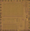
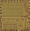
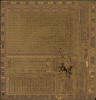
The TMC0580 was manufactured in a 6 um metal gate PMOS process (metal width = 0.25 mil / 6.0 um, metal spacing = 0.30 mil / 8.0 um, diffusion width = 0.25 mil / 6.0 um, diffusion spacing = 0.30 mil / 8.0 um).
The die size of the TMC0580 is approximately 215 mils * 220 mils / 5.4 mm * 5.6 mm.
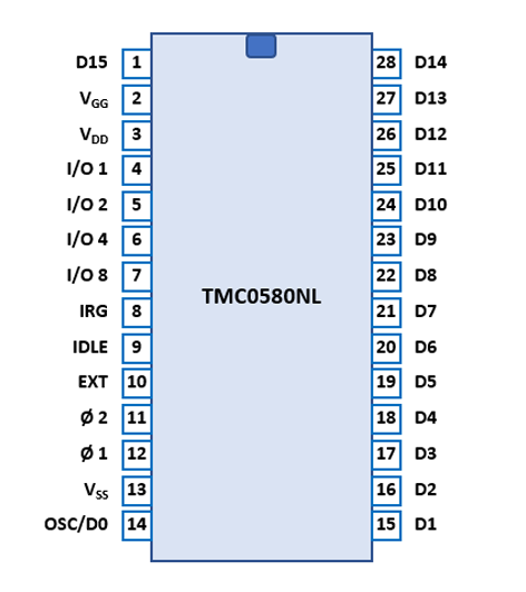
The TMC0580 uses a 0.4” wide 28-pin SPDIP (Shrink Plastic Dual In-line Package with a 0.07” / 1.778 mm lead pitch).
| Pin | IO | Function | Pin | IO | Function |
| 1 | O | Digit driver 15 | 28 | O | Digit driver 14 |
| 2 | V | Negative Voltage VGG | 27 | O | Digit driver 13 (OVER) |
| 3 | V | Negative Voltage VDD | 26 | O | Digit driver 12 (M-MSD) |
| 4 | IO | SCOM Interface D0 | 25 | O | Digit driver 11 |
| 5 | IO | SCOM Interface D1 | 24 | O | Digit driver 10 |
| 6 | IO | SCOM Interface D2 | 23 | O | Digit driver 9 |
| 7 | IO | SCOM Interface D3 | 22 | O | Digit driver 8 |
| 8 | O | Instruction words | 21 | O | Digit driver 7 |
| 9 | I | Calculating status | 20 | O | Digit driver 6 |
| 10 | I | External access | 19 | O | Digit driver 5 |
| 11 | I | Clock Input 2 | 18 | O | Digit driver 4 |
| 12 | I | Clock Input 1 | 17 | O | Digit driver 3 (M-LSD) |
| 13 | V | Common Voltage | 16 | O | Digit driver 2 (E-MSD) |
| 14 | XO | Oscillator/Digit driver 0 | 15 | O | Digit driver 1 (E-LSD) |
The keyboards of all calculators based on the TMC0501E Arithmetic chip consist of an x/y-matrix connected to the SCOM digit driver outputs and the TMC0501E keymatrix inputs.
Example for the SR-51-II with TMC0581:
| KN | KO | KP | KQ | KR | KS | KT | |
| D5 | 2nd | sin | cos | tan | CLR | ||
| D7 | INV | % | lnx | eX | x√y | ||
| D3 | x<>y | x2 | √x | 1/x | yX | ||
| D4 | ∑+ | EE | ( | ) | ÷ | ||
| D2 | STO | 7 | 8 | 9 | × | ||
| D1 | RCL | 4 | 5 | 6 | − | ||
| D8 | SUM | 1 | 2 | 3 | + | ||
| D6 | CE | 0 | . | +/− | = |
Example for the TI-58 and TI-59 with TMC0582:
| KN | KO | KP | KQ | KR | KS | KT | |
| D0 | [PC100] | (1) | |||||
| D1 | A | B | C | (1) | D | E | |
| D2 | 2nd | INV | lnx | (1) | CE | CLR | |
| D3 | LRN | x<>t | x2 | (1) | √x | 1/x | |
| D4 | SST | STO | RCL | (1) | SUM | yX | |
| D5 | BST | EE | ( | (1) | ) | ÷ | |
| D6 | GTO | 7 | 8 | (1) | 9 | × | |
| D7 | SBR | 4 | 5 | [58] | 6 | − | |
| D8 | RST | 1 | 2 | (1) | 3 | + | |
| D9 | R/S | 0 | . | (1) | +/− | = | |
| D10 | [CS] | ||||||
| D11 | (1) | ||||||
| D12 | (ADV) | (PRT) | (1) | ||||
| D13 | (1) | ||||||
| D14 | (1) | ||||||
| D15 | [TRC] | (1) |
Notes: The TI-58 is identified by a diode between D7 - KR, the TI-59 detects the Card Sense switch between D10 - KR. The PC-100A is detected by a diode between D0 - KP and the (PRT), (ADV) and [TRC] nodes are used to detect PRINT, PAPER ADVANCE and TRACE on the Printer Cradle PC-100. The BUSY output of the TMC0251 Printer/Display Chip used with the PC-100A/PC-100B/PC-100C is connected to KR(1) and consequently active during all 16 Digit Times D0 to D15.
Example for the TI-5230 with TMC0587:
| KN | KO | KP | KQ | KR | KS | KT | |
| D0 | (1) | (2) | |||||
| D1 | TAPE ADV |
TAPE ON/OFF |
(1) | (2) | LIST | ||
| D2 | SET UP |
START | (1) | (2) | STOP | ENTER | |
| D3 | DR | CR | (1) | (2) | CONST | CA | |
| D4 | LINE | COL | (1) | (2) | MODE | C/CE | |
| D5 | 7 | 4 | (1) | (2) | 1 | 0 | |
| D6 | 8 | 5 | (1) | (2) | 2 | 00 | |
| D7 | 9 | 6 | (1) | (2) | 3 | . | |
| D8 | − | (1) | (2) | + | |||
| D9 | N | GT | (1) | (2) | #/S | T | |
| D10 | % | ÷ | (1) | (2) | × | = | |
| D11 | CM | RM | (1) | (2) | M−= | M+= | |
| D12 | [DP S] | (1) | (2) | ||||
| D13 | [PROT] | (1) | (2) | ||||
| D14 | (1) | (2) | |||||
| D15 | (1) | (2) |
Notes: The DECIMAL SET switch of the TI-5230 is detected with a diode between D12 - KN and its PROTECT switch with a diode between D13 - KN. The power supply of the TMC1376 Display Controller is detected with KQ(1) (Display Off = active) and KR(2) is connected to the BUSY Output of the TMC0255 Printer/Display Chip (Busy = active).
If you have additions to the above datasheet please email: joerg@datamath.org.
© Joerg Woerner, February 02, 2001. No reprints
without written permission.