DATAMATH CALCULATOR MUSEUM
|
DATAMATH CALCULATOR MUSEUM |
Texas Instruments announced on September 16, 1975 with the SR-52 their first Keystroke Programmable Handheld Calculator based on the TMS0500 Building Blocks for Scientific and Programmable Calculators introduced already in January 1974 with the SR-50 “Slide Rule” calculator. While the SR-50 used only the minimum configuration of this groundbreaking architecture combining the TMC0501 Arithmetic Chip and one TMC0521 SCOM (Scanning Read-Only Memory) Chip with the necessary display drivers for its 14-digit LED display plus power supply and clock generation, went the SR-52 a step ahead and made full use of the TMS0500 Building Blocks. The TI Programmable 59 – nicknamed SR-52 II - was introduced in May 1977 as successor of the SR-52 and perfectly applied Moore’s Law integrating more memory capacity in smaller packages while lowering complexity. A closer look at the PCB (printed circuit board) of the TI-59 reveals a total of nine PMOS (P-channel Metal–oxide Semiconductor) chips:
|
• TMC0501E: Enhanced Arithmetic Chip – Register Processor with five 16-digit Registers and segment decoder/driver • TMC0582, TMC0583: TMC0580 Double Scanning and Read-Only Memory Chip – 2.5k*13 Bits Instruction Memory with serial interface to Arithmetic Chip, 32 Constants with 16 digits, eight 16-digit Registers and 16-digit display scanning, each • TMC0571: TMC0560 Bare Read-Only Memory Chips – 1k*13 Bits Instruction Memory with serial interface to Arithmetic Chip for a combined 6k*13 Bits Instruction Memory • TMC0594: Magnetic I/O Chip – Four channel interface for magnetic card reader to save and load programs with up to 480 steps • TMC0598*4: Four Multi-Register Chips – 240*8 Bits Random Access Memory with 4-bit I/O Bus to Arithmetic Chip, stores 240 program steps or 30 numbers of 16 digits, each |
The TMC0598 Multi-Register Chip integrates 240*8 Bits RAM (Random Access Memory) storing 240 program steps or 30 numbers of 16 digits, each and accessible through a 4-bit bidirectional I/O bus. The design of the TMC0598 with one Chip Select (C.S.) and two Address pins (ADD0, ADD 1) allows for both compact designs with stacking two by two chips, each in a piggyback manner with cutting one of the two Address pins and large designs with an external address decoder activating the Chip Select pin:
| Address | TMC0598 Stack 1 | TMC0598 Stack 2 | ||
| Chip Position | Top Chip | Bottom Chip | Top Chip | Bottom Chip |
| ADD 0 | n.c. | VSS | n.c. | VSS |
| ADD 1 | n.c. | n.c. | VSS | VSS |
| C.S. | n.c. | n.c. | n.c. | n.c. |
| Active Bank | Bank 0 | Bank 1 | Bank 2 | Bank 3 |
Communication between the TMC0501E
Enhanced Arithmetic Chip to the TMC0598 Multi-Register Chip is realized with multiple means:
|
• IDLE, PHI 1 and PHI 2
Signals are used to synchronize all peripherals connected to the TMC0501E
Enhanced Arithmetic Chip with the 16 States of its Instruction Cycle • EXT Output indicates that the TMC0501E Enhanced Arithmetic Chip is addressing external memories/registers • IRG Input to receive the 13-bit Instruction Words from the TMC0530/TMC0540/TMC0560/TMC0580 ROM Chips • 4-bit bidirectional I/O Bus I/O 8, I/O 4, I/O 2, and I/O 1 to communicate with registers |
QUICK-LINK to TMS0500 Family.
| Calculator | Program steps | Data memory | TMC0599 |
| TI-58 | 0-480 | 60-0 | 2 |
| TI-59 | 160-960 | 100-0 | 4 |
| TI-5230 | t.b.d. | t.b.d. | 7 |
| Revision | Products | First Prototypes | Comments |
| TMC0598 | SR-52 II (TI-59) | November 1976 | Initial design Formerly TMC0599 Rev E |
| Item | Min | Typ | Max | Unit | Comments |
| VSS | 0 | V | |||
| VDD | -10.5 | -10.0 | -9.5 | V | |
| PHI1, PHI2 | 225 | 230 | kHz | Opposite phases |
The TMC0598 was manufactured in a 8 um metal gate PMOS process (metal width = 0.30 mil / 8.0 um, metal spacing = 0.30 mil / 8.0 um, diffusion width = 0.25 mil / 6.0 um, diffusion spacing = 0.35 mil / 9.0 um).
The die size of the TMC0598 is approximately 210 mils * 140 mils / 5.3 mm * 3.6 mm.
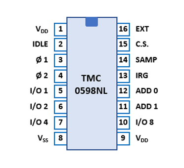
The TMC0598 uses a standard 0.3” wide 16-pin DIP (Dual In-line Package with a 0.1” / 2.54 mm lead pitch).
| Pin | IO | Function | Pin | IO | Function |
| 1 | V | Negative Voltage VDD | 16 | I | External access |
| 2 | I | Calculating status | 15 | I | CS (not connected) |
| 3 | I | Clock Input 1 | 14 | I | SAMP (not connected) |
| 4 | I | Clock Input 2 | 13 | O | Instruction words |
| 5 | IO | SCOM Interface D0 | 12 | I | Bank-Select 1 (VSS, nc) |
| 6 | IO | SCOM Interface D1 | 11 | I | Bank-Select 0 (VSS, nc) |
| 7 | IO | SCOM Interface D2 | 10 | IO | SCOM Interface D3 |
| 8 | V | Common Voltage | 9 | V | Negative Voltage VDD |
If you have additions to the above datasheet please email: joerg@datamath.org.
© Joerg Woerner, February 02, 2001. No reprints
without written permission.