DATAMATH CALCULATOR MUSEUM
|
|
DATAMATH CALCULATOR MUSEUM |
Datamath Calculator Museum DCM-0500 (Platform)
| Date of introduction: | January 15, 2024 | Display technology: | |
| New price: | $1,049.95 (2022 = $169.95 in 1974) | Display size: | |
| Size: | 4.0" x 13.2" x 1.7" 102 x 335 x 43 mm3 |
||
| Weight: | 11.4 ounces, 323 grams | Serial No: | 0001 |
| Batteries: | Date of manufacture: | mth 01 year 2024 | |
| AC-Adapter: | DC 5V (USB) | Origin of manufacture: | USA |
| Precision: | Integrated circuits: | ZIF-Sockets for TMC0520, TMC0530, TMC0540, TMC0560, TMC0580 | |
| Memories: | Displays: | ||
| Program steps: | Courtesy of: | Joerg Woerner |
![]() When Hewlett-Packard formally introduced on January 4th, 1972 its
revolutionary HP-35, it seemed to be far ahead of the four bangers like Bowmar's
Model 901B based on Texas
Instruments' "calculator-on-a-chip"
technology introduced just 3 months earlier with the
TMS1802, later rebranded as TMS0102. And
Hewlett-Packard indeed designed the HP-35 based on a multi-chip architecture
using five separate chips, each with a complexity of around 5,000 transistors
comparable to the TMS1802 and manufactured by either Mostek Corp., Carrollton, TX or American Microsystems Inc., Santa Clara, CA.
Texas Instruments was no stranger to multi-chip architectures, more or less in
parallel with the TMS1802 they worked for Canon on the TMC1813/TMC1814 chipset
for their Canola L121F Desktop
calculator leading directly into the
TMS0200 Building Blocks for Desktop
Calculators. They are centered around the TMS0200
Data Chip, TMS0300 ROM (Read-Only Memory)
Chip and TMC0400 ROM/Register Chip. But
each of the three Chips was encapsulated in a large 40-pin Dual In-line Package
(DIP) making them unsuitable for a handheld product.
When Hewlett-Packard formally introduced on January 4th, 1972 its
revolutionary HP-35, it seemed to be far ahead of the four bangers like Bowmar's
Model 901B based on Texas
Instruments' "calculator-on-a-chip"
technology introduced just 3 months earlier with the
TMS1802, later rebranded as TMS0102. And
Hewlett-Packard indeed designed the HP-35 based on a multi-chip architecture
using five separate chips, each with a complexity of around 5,000 transistors
comparable to the TMS1802 and manufactured by either Mostek Corp., Carrollton, TX or American Microsystems Inc., Santa Clara, CA.
Texas Instruments was no stranger to multi-chip architectures, more or less in
parallel with the TMS1802 they worked for Canon on the TMC1813/TMC1814 chipset
for their Canola L121F Desktop
calculator leading directly into the
TMS0200 Building Blocks for Desktop
Calculators. They are centered around the TMS0200
Data Chip, TMS0300 ROM (Read-Only Memory)
Chip and TMC0400 ROM/Register Chip. But
each of the three Chips was encapsulated in a large 40-pin Dual In-line Package
(DIP) making them unsuitable for a handheld product.
Being already late, Texas Instruments knew that they needed to be better than their competition and they analyzed the hot-selling HP-35 carefully to identify some weaknesses of its design:
|
• RPN (Reverse Polish Notation)
is very efficiently implemented in a scientific calculator, but for the average user it might be prohibitive • While the HP-35 was the first portable electronic calculator featuring transcendental functions, does it lack hyperbolic functions • Using a bit-serial architecture, the algorithm used to implement the transcendental functions were a tradeoff of accuracy and speed • And last but not least the US$ 395 price tag |
Various teams at Texas Instruments were addressing each of these bullet points and the SR-50 was their answer! The calculator was formally introduced on January 15th, 1974 and here at the Datamath Calculator Museum we celebrate its groundbreaking architecture defining the TMS0500 Building Blocks for Scientific and Programmable Calculators with this DCM-0500 Platform accordingly! While we considered in Summer 2023 the idea of designing a calculator platform for the TMS0500 Building Blocks similar to the DMC-50A, contacted us a member of the TI-59 Community and shared his misery with us and we changed gears immediately. Learn more about the Birth of the DCM-0500. Breadboarding a fully functional SR-60A might be a retirement project.
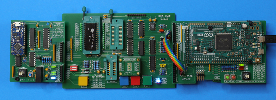
With the TMS0500 Building Blocks designed exclusively for Texas Instruments' proprietary applications and never made available to OEM manufacturers, available documentation of their features is rather scarce and the Datamath Calculator Museum is committed to fill this gap with "Data Sheets" for the individual components. The modular approach of the TMS0500 architecture is centered around an Arithmetic Chip and at least one so-called Scanning ROM (Read-Only Memory) Chip necessary for a minimum configuration and expandable with different Peripheral Chips like Magnetic I/O Chip, Multi-Register Chips and Printer/Display Chips. A novelty introduced with the TI Programmable 59 are the Solid State Software Modules™ containing up to 5,000 program steps and inserted into the backside of the calculators. From a technical point of view is most of the calculator functionality defined with the various ROM Chips of the TMS0500 Building Blocks, namely the TMC0520 Scanning ROM, its successor TMC0530 Scanning ROM, TMC0580 Double Scanning ROM, TMC0560 Bare ROM and TMC0540 Customer ROM. To provide enthusiasts as much information as possible about calculators based on the TMC0501 Arithmetic Chip or TMC0501E Enhanced Arithmetic Chip, we developed the DCM-0500 Platform to allow Recording of ROM Images of the Integrated Circuits (ICs) used with these designs.
Reverse-engineering of Calculators
Without official data sheets about the individual products of the TMS0500 Building Blocks available, we not only studied schematics, service manuals and patent applications of different calculators, but utilized the art of reverse-engineering with some of the components used with the calculators. Reverse-engineering of a single component in a product is basically a 4-step approach:
| • Observe - Dismantle the
product and get an idea how the component is used in its environment • Analyze - Look closely into the operation of the component to understand its function • Model - Create a replacement of the component based on the gained understanding • Deploy - Use the designed new component for the intended application |
Understanding that a product based on the TMS0500 Building Blocks uses always one Arithmetic Chip but could employ multiple different ROM Chips, we centered the DMC-0500 around a TMS0500 ROM Platform and added various connectors supporting all aspects of reverse-engineering necessary to retrieve the stored Bits and Bytes of these ROM Chips.
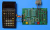
Observe: The first step in reverse-engineering of calculators centered around the TMS0500 Building Blocks is accessing the relevant signals within a certain product of interest, we typically use the SR-50 as "Minimum Configuration Calculator" and the TI-58 as "Maximum Configuration Calculator", the SR-51 to explore the use of Constants and the SR-51-II to dig into the undocumented Key Codes for calculators other than the TI-58, TI-58C, and TI-59. Looking closely into the communication between the TMC0501 Arithmetic Chip and TMC0521 Scanning Read-Only Memory used with the SR-50 and SR-50A, you understand that there are four signal groups from interest:
|
• IDLE, PHI 1 and PHI 2
Signals are used to synchronize the TMC0521 with the 16 States of the
TMC0501 Instruction Cycle • EXT Output indicates that the TMC0501 is addressing external Instruction Memories or Constant Registers • IRG Input to receive the 13-bit Instruction Words from the TMC0521 • 4-bit bidirectional I/O Bus I/O 8, I/O 4, I/O 2, and I/O 1 to read in Constants from the TMC0521 |
 The TMS0500 ROM Platform is
providing on the West-Port consequently a 10-pin connector for these 9 signals
plus an additional GND pin to wire the respective signals of the calculator
under Observation accordingly. A second 8-pin connector at the West-Port
provides a DC Voltage to power the calculator connected to the TMS0500 ROM
Platform, to allow looking into Power-On behavior of the connected calculator,
the DC Voltage is provided either momentarily by the Yellow [CALC] push button
or using the Red rocker switch. Additionally the 8-pin connector carries the
various voltages used within the Integrated Circuits (ICs) of the TMS0500
Building Blocks, namely VSS (0 V), VDD (-10 V) and VGG (-15.8 V)
and connected to the ZIF-Sockets of the TMS0500 ROM Platform.
The TMS0500 ROM Platform is
providing on the West-Port consequently a 10-pin connector for these 9 signals
plus an additional GND pin to wire the respective signals of the calculator
under Observation accordingly. A second 8-pin connector at the West-Port
provides a DC Voltage to power the calculator connected to the TMS0500 ROM
Platform, to allow looking into Power-On behavior of the connected calculator,
the DC Voltage is provided either momentarily by the Yellow [CALC] push button
or using the Red rocker switch. Additionally the 8-pin connector carries the
various voltages used within the Integrated Circuits (ICs) of the TMS0500
Building Blocks, namely VSS (0 V), VDD (-10 V) and VGG (-15.8 V)
and connected to the ZIF-Sockets of the TMS0500 ROM Platform.
Observation of the serial IRG and EXT signals is usually performed with a Digital Oscilloscope or Logic Analyzer, here at the Datamath Calculator Musuem we rely on our Hewlett-Packard 54645D Mixed Signal Oscilloscope, Agilent 1672G Logic Analyzer and Digilent Digital Discovery. While these devices are typically connected to modern electronics powered by voltages in the range of 3 Volts to 5 Volts, are the TMS0500 chips manufactured in a 8 um metal gate PMOS process requiring two voltages of -10.0 Volts and -15.8 Volts. The TMS0500 ROM Platform is providing level-shifters to 5 Volts for all PMOS signals connected to the West-Port. Another difficulty observing the serial IRG and EXT signals was introduced with Texas Instruments' desire to keep the pin count of the various ICs as low as possible and engineers chose to combine two functions with the IDLE signal:
|
• Synchronizing all
peripherals connected to the TMC0501/TMC0501E Arithmetic Chips with the
16 States of its Instruction Cycle • Signaling the power supply and peripherals if the TMC0501/TMC0501E is in "Calculating" or "Displaying" mode |
To allow an easier synchronization of data capturing with Digital Oscilloscopes or Logic Analyzers includes the TMS0500 ROM Platform a "State Counter" signaling the S0 State of the TMS0501/TMC0501E Chips connected to its East-Port. The 10-pin connector of the North-Port of the TMS0500 ROM Platform labeled "DEBUG INTERACE" is providing three signal groups from the West-Port, the S0 State signal in 5 Volt CMOS Level and an additional GND pin for easy observation of the connected calculator:
|
• IDLE, PHI 1 and PHI 2 • EXT • IRG • State S0 |
Analyze: The second step in reverse-engineering of calculators centered around the TMS0500 Building Blocks is understanding the relevant signals of the component from interest and while both Digital Oscilloscopes and Logic Analyzers are handy tools used in Observation, do they usually lack both functionality and comfort in Analyzing the signals. Looking into the power-up behavior of a SR-50 with an Digital Oscilloscope might be overwhelming, after executing a few instructions to initialize internal registers, the TMC0501/TMS0501E Arithmetic Chip is waiting for a pushed key on the keyboard, effectively generating tens of thousands of serial signals per second. In Software Development for Embedded Microcontroller Architectures one important step is called Debugging and there are different approaches between Trial-and-Error and Test-Bench methodology. One commonly used tool is a "Debugger" that connects to the relevant signal of the Microcontroller and allows "Trigger Conditions", e.g. access to a certain memory location on the Address-Bus or certain data content on the Data-Bus. With the TMS0500 Building Blocks based on a serial Register Processor, we followed an approach to de-serialize the relevant signals into parallel 16-bit words, make them available to an Arduino board and develop "TMS0500 DATA Recorder" Software running on a Arduino DUE simply logged the information from the IRG and EXT signals and the I/O Bus and listing them it in a human readable form in a terminal window. The necessary electronics is connected to the East-Port of the TMS0500 ROM Platform and consist of two modules:
|
• Bottom: TMS0500 8-Channel Serial Data Recorder 128-Bit Module • Top: TMS0500 8-Channel Serial Data Recorder with Arduino DUE |
The TMS0500 8-Channel Serial Data Recorder 128-Bit Module is basically and arrangement of eight 16-bit Serial-to-Parallel Shift Registers, for the TMS0500 Building Blocks only six channels are used:
|
• Channel 1: EXT Signal • Channel 2: IRG Signal • Channel 3: not used • Channel 4: not used • Channel 5: I/O 1 Signal • Channel 6: I/O 2 Signal • Channel 7: I/O 4 Signal • Channel 8: I/O 8 Signal |
![]() While the TMS0500 Building Blocks uses a digit-serial
architecture representing numbers in 16*4 bits are other calculator
architectures using different approaches, Hewlett-Packard decided for example
with its HP-35 with for a bit-serial architecture representing numbers in 56
bits. The TMS0500 8-Channel Serial Data Recorder 128-Bit Module allows not only
for reconfiguration of its 128-Bit Shift Registers into eight 16-Bit channels,
four 32-Bit channels, two 64-bit channels or one 128-Bit channel, up to eight of
the Modules can be stacked in a piggy-back manner for a combined 1024-Bit Module.
While the TMS0500 Building Blocks uses a digit-serial
architecture representing numbers in 16*4 bits are other calculator
architectures using different approaches, Hewlett-Packard decided for example
with its HP-35 with for a bit-serial architecture representing numbers in 56
bits. The TMS0500 8-Channel Serial Data Recorder 128-Bit Module allows not only
for reconfiguration of its 128-Bit Shift Registers into eight 16-Bit channels,
four 32-Bit channels, two 64-bit channels or one 128-Bit channel, up to eight of
the Modules can be stacked in a piggy-back manner for a combined 1024-Bit Module.
The TMS0500 8-Channel Serial Data Recorder is mounted on top of the TMS0500 8-Channel Serial Data Recorder 128-Bit Module (or stack of multiple 128-Bit Modules) and consists of two components:
|
• Base-Board: "User
Interface" and optional 8-MBit Memory Expansion for Arduino DUE • Arduino DUE: 32-bit ARM core microcontroller, 96k Bytes Data Memory, 512k Bytes, I/Os and USB Interface |
![]() Main
application on the Arduino DUE is the "TMS0500 DATA Recorder" Software that
allows the definition of various trigger conditions for logging IRG and EXT
signals and the I/O Bus like "Address Match" and "Data Match" with 0,1,X
qualifiers, pre-trigger and post-trigger logging and and storing the
information in a human readable form. With this powerful tool we logged for
example how the TI-58 accesses its Solid State Software Module when performing a
simple "Master Library" function, how a SR-51A is accessing its Constant ROM
when converting from inches to millimeters or what values the 16 constants with
13-digit precision used with the computing algorithm of trigonometric functions
like sine, cosine, or tangent actually have. The user interface of the "TMS0500
DATA Recorder" Software is rather simple, a 16-position rotary switch selects
the desired program, a green [INIT] button starts it and a red [STOP] button
resets the system. The
"Recording" in the Arduino DUE software includes:
Main
application on the Arduino DUE is the "TMS0500 DATA Recorder" Software that
allows the definition of various trigger conditions for logging IRG and EXT
signals and the I/O Bus like "Address Match" and "Data Match" with 0,1,X
qualifiers, pre-trigger and post-trigger logging and and storing the
information in a human readable form. With this powerful tool we logged for
example how the TI-58 accesses its Solid State Software Module when performing a
simple "Master Library" function, how a SR-51A is accessing its Constant ROM
when converting from inches to millimeters or what values the 16 constants with
13-digit precision used with the computing algorithm of trigonometric functions
like sine, cosine, or tangent actually have. The user interface of the "TMS0500
DATA Recorder" Software is rather simple, a 16-position rotary switch selects
the desired program, a green [INIT] button starts it and a red [STOP] button
resets the system. The
"Recording" in the Arduino DUE software includes:
|
• A: Trace ALL (Store all
information recorded on IRG, EXT and I/O Bus) • B: Trace TRG (Store information recorded on IRG, EXT and I/O Bus after trigger conditions are met) • C: Trace TRG+ (Store information recorded on IRG, EXT and I/O Bus before and after trigger conditions are met) |
Model: Understanding the TMS0500 Building Blocks gained through intensive Observation and Analysis of the relevant signals and information allows in a third step to create replacements of the individual components of the calculator. With most of the calculator functionality defined with the various ROM Chips of the TMS0500 Building Blocks, our focus is clearly on Recording of ROM Images and the easiest way to access their content is to "Emulate" a TMC0501/TMC0501E Arithmetic Chip while accessing the respective ROMs. The TMS0500 Building Blocks define three different types of ROMs:
|
• First ROM: Used for Instruction
Memory - TMC0520, TMC0530, TMC0560 and TMC0580 • Second ROM: Used for Key Codes - TMC0540 (Solid State Software Modules) • Constant ROM: Used for Constants - TMC0520, TMC0530 and TMC0580 or Key Codes - TMC0530 and TMC0580 |
To access the information stored during the manufacturing process of the various ROM Chips, the TMC0501/TMC0501 Arithmetic Chips are using the four signal groups mentioned earlier:
|
• IDLE, PHI 1 and PHI 2
Signals are used to synchronize all peripherals connected to the TMC0501/TMC0501E Arithmetic Chips with the 16 States of its Instruction Cycle • EXT Output indicates that the TMC0501/TMC0501E Arithmetic Chips is addressing external memories/registers • EXT Input to receive 2-digit BCD Key Codes (8-bit) from the TMC0540 CROM Chips • IRG Input to receive the 13-bit Instruction Words from the TMC0520/TMC0530/TMC0560/TMC0580 ROM chips • 4-bit bidirectional I/O Bus I/O 8, I/O 4, I/O 2, and I/O 1 to communicate with Multi-Register Chips and other peripherals |
The TMC0501/TMC0501E Emulator uses a software approach to stimulate the signals used with the various ROMs using an Arduino Nano Every running different programs selected with a rotary switch, level-shifters from the 5 Volt Outputs of the Arduino microcontroller to the PMOS levels used with the ROMs and a DC/DC converter to provide the voltages used with the TMS0500 Building Blocks, namely VSS (0 V), VDD (-10 V) and VGG (-15.8 V). The user interface of the TMC0501/TMC0501E Emulator is pretty simple, the rotary switch selects one of 3 programs and a blue [PLAY] button starts the program and enables the level-shifters for the various output signals. The "Playlist" in the Arduino Nano Every software includes:
|
• 0-7: Access First ROM Bank
0 to 7 of the TMS0500 Building Blocks (1,024 13-bit Instruction Words,
each) • 8: Access Second ROM of the TMS0500 Building Blocks (5,000 2-digit BCD Key Codes) • 9: Access Constant ROM of the TMS0500 Building Blocks (8*16 16-digit Constants) |
The TMC0501/TMC0501E Emulator is compatible with the West-Port of the TMS0500 ROM Platform and can substitute the physical calculators for the purpose of Recording of ROM Images from its ZIF-Sockets.
Deploy: The TMC0501/TMC0501E Emulator allows to stimulate the various ROMs used with the TMS0500 Building Blocks to reveal their stored information and the TMS0500 8-Channel Serial Data Recorder allows logging of the respective responses of the ROMs. Together with the various ZIF-Sockets provided on the the TMS0500 ROM Platform it just takes some coordinated software running on the two Arduino Platforms for Recording of ROM Images. In the "Deploy Configuration" the Arduino DUE is running the "TMS0500 ROM Recorder" Software not only logging the information from the IRG and EXT signals and the I/O Bus but transcribing them into actual ROM listings including Address and Data information.
The user interface of the "TMS0500 ROM Recorder" Software is rather simple, a 16-position rotary switch selects the desired program, a green [INIT] button starts it and a red [STOP] button resets the system. The "Recording" in the Arduino DUE software includes:
|
• 0-7: Record First ROM Bank
0 to 7 of the TMS0500 Building Blocks (1,024 13-bit Instruction Words,
each) • 8: Record Second ROM of the TMS0500 Building Blocks (5,000 2-digit BCD Key Codes) • 9: Record Constant ROM of the TMS0500 Building Blocks (8*16 16-digit Constants) |
![]() The two Arduino Platforms use a handshake to synchronize their
program flow and a typical "Recording Session" consist of just seven steps
after connecting the Arduino DUE of the TMS0500 8-Channel Serial Data Recorder
to a USB Port of a
PC or Laptop and starting a Terminal Program:
The two Arduino Platforms use a handshake to synchronize their
program flow and a typical "Recording Session" consist of just seven steps
after connecting the Arduino DUE of the TMS0500 8-Channel Serial Data Recorder
to a USB Port of a
PC or Laptop and starting a Terminal Program:
|
• 1: Insert ROM into
corresponding ZIF-Socket of the TMS0500 ROM Platform • 2: Select desired ROM Type on "Playlist" of the TMC0501/TMC0501E Emulator • 3: Select desired ROM Type on 'Recording" of the TMS0500 8-Channel Serial Data Recorder • 4: Push the green [INIT] button on the TMS0500 ROM Platform to clear all buffers and registers • 5: Push the blue [PLAY] button on the TMS0500 ROM Platform to initiate the selected "Playlist". Blue LED signals that the ZIF-Sockets is "LIVE" • 6: "Recording" will start automatically and red LED signals "RECORD". End of recording session is signaled with the red LED turning off. Blue LED turning off signals that it is safe to remove the ROM • 7: Review the recorded ROM Image |
Texas Instrument introduced on January 15th, 1974 with the SR-50 their first product based on the the TMS0500 Building Blocks for Scientific and Programmable Calculators. The SR-50 used with the TMC0501 Arithmetic Chip and TMC0521 Scanning ROM Chip only the bare minimum of its possibilities but the subsequent introduction of the SR-52 Programmable and the PC-100 Printer Cradle clearly demonstrated the scalability of this groundbreaking architecture. While from a technology point of view the SR-60A Prompting Calculator marked the eclipse of the TMS0500 Building Blocks, was it the TI Programmable 59 that will be remembered for eternity.
With most of the calculator functionality defined with the various ROM Chips of the TMS0500 Building Blocks, our focus hear at the Datamath Calculator Museum is clearly on Recording of ROM Images and the easiest way to access their content is to "Emulate" the TMC0501/TMC0501E Arithmetic Chip while accessing the respective ROMs. The TMS0500 Building Blocks define three different types of ROMs:
|
• First ROM: Used for Instruction
Memory - TMC0520, TMC0530, TMC0560 and TMC0580 • Second ROM: Used for Key Codes - TMC0540 (Solid State Software Modules) • Constant ROM: Used for Constants - TMC0520, TMC0530 and TMC0580 or Key Codes - TMC0530 and TMC0580 |
In 1965, Gordon E. Moore - co-founder of Intel - postulated that the number of transistors that can be packed into a given unit of space will double about every two years. This allowed to integrate more and more transistors, diodes and resistors into Integrated Circuits and consequently the capacity of the ROMs changed over time:
|
• First ROM: TMC0520, TMC0530
and TMC0560 (1,024 13-bit Instruction Words), TMC0580 (2,560 13-bit
Instruction Words) • Second ROM: TMC0540 (5,000 2-digit BCD Key Codes) • Constant ROM: TMC0520 and TMC0530 (16 16-digit Constants), TMC0580 (32 16-digit Constants) |
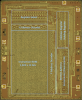 The ROM (Read-Only Memory) Chips used within the TMS0500
Building Blocks are manufactured with an 8 um (early designs) or 6 um (later
designs) metal gate PMOS process where the information in the form of the
individual Bits that make up a 13-bit Instruction Word, a 2-digit BCD Key Code
(8-bit) or 16-digit Constants (64-bit) are stored in the layout of the Chips
using a single metal mask. Decapping the chips and photographing them under a
microscope makes the individual Bits actually visible and with some additional
smart software tools the data content can be retrieved. One of the disadvantages
of this brute force method is its destructive character, hence did we develop
here at the Datamath Calculator Museum with the DCM0500 Platform an approach to
Record the stored ROM Images electronically.
The ROM (Read-Only Memory) Chips used within the TMS0500
Building Blocks are manufactured with an 8 um (early designs) or 6 um (later
designs) metal gate PMOS process where the information in the form of the
individual Bits that make up a 13-bit Instruction Word, a 2-digit BCD Key Code
(8-bit) or 16-digit Constants (64-bit) are stored in the layout of the Chips
using a single metal mask. Decapping the chips and photographing them under a
microscope makes the individual Bits actually visible and with some additional
smart software tools the data content can be retrieved. One of the disadvantages
of this brute force method is its destructive character, hence did we develop
here at the Datamath Calculator Museum with the DCM0500 Platform an approach to
Record the stored ROM Images electronically.
The DCM-0500 Platform is designed with individual modules that can be configured and customized for different purposes, for the Recording of ROM Images we use the "Deploy Configuration" with four modules:
|
• TMS0500 ROM Platform: Center-piece with ZIF-Sockets
for TMC0520, TMC0530, TMC0540, TMC0560, TMC0580 Chips and optional
SSSM Adapter • TMC0501/TMC0501E Emulator connected to the West-Port of the TMS0500 ROM Platform to stimulate the ROM Chips • One TMS0500 8-Channel Serial Data Recorder 128-Bit Module connected to the East-Port of the TMS0500 ROM Platform to convert the bit- and digit-serial responses of the ROM Chips into parallel 16-bit words • TMS0500 8-Channel Serial Data Recorder in Basic Configuration piggy-backed to the East-Port of the TMS0500 ROM Platform to convert the ROM responses into actual ROM listings |
The Recorded ROM Images of the various ROM Chips used within the TMS0500 Building Blocks for Scientific and Programmable Calculators are published as TXT-Files in the "ROM Content" sections of their respective "Data Sheets":
|
•
TMC0520: Instruction
ROM and Constant ROM of SR-50, SR-51, SR-51A, SR-52 • TMC0530: Instruction ROM and Constant ROM of SR-50A, SR-51A, SR-52A, SR-56 and Disassembled Key Code Program of SR-56 • TMC0540: Key Code ROM and Disassembled Key Code Programs of 25 different Solid State Software Modules™ • TMC0560: Instruction ROM of PC-100, SR-52, TI-58C, TI-59 • TMC0580: Instruction ROM and Constant ROM of SR-51-II, TI-58C, TI-59 and Disassembled Key Code Program of TI-58C, TI-59 |
IMPORTANT NOTE: This information is provided as a service of the Datamath Calculator Museum to enthusiasts of early Texas Instruments calculators and please be aware that the Copyright of the Software transcribed in the ROM Images, the underlying algorithm or application might be owned by Texas Instruments or other third parties. The commercial use of the published Recorded ROM Images is strictly prohibited. In case of questions please contact us using the email address listed in the footer of this webpage.
If you have additions to the above article please email: joerg@datamath.org.
© Joerg Woerner, January 15, 2024. No reprints without written permission.